

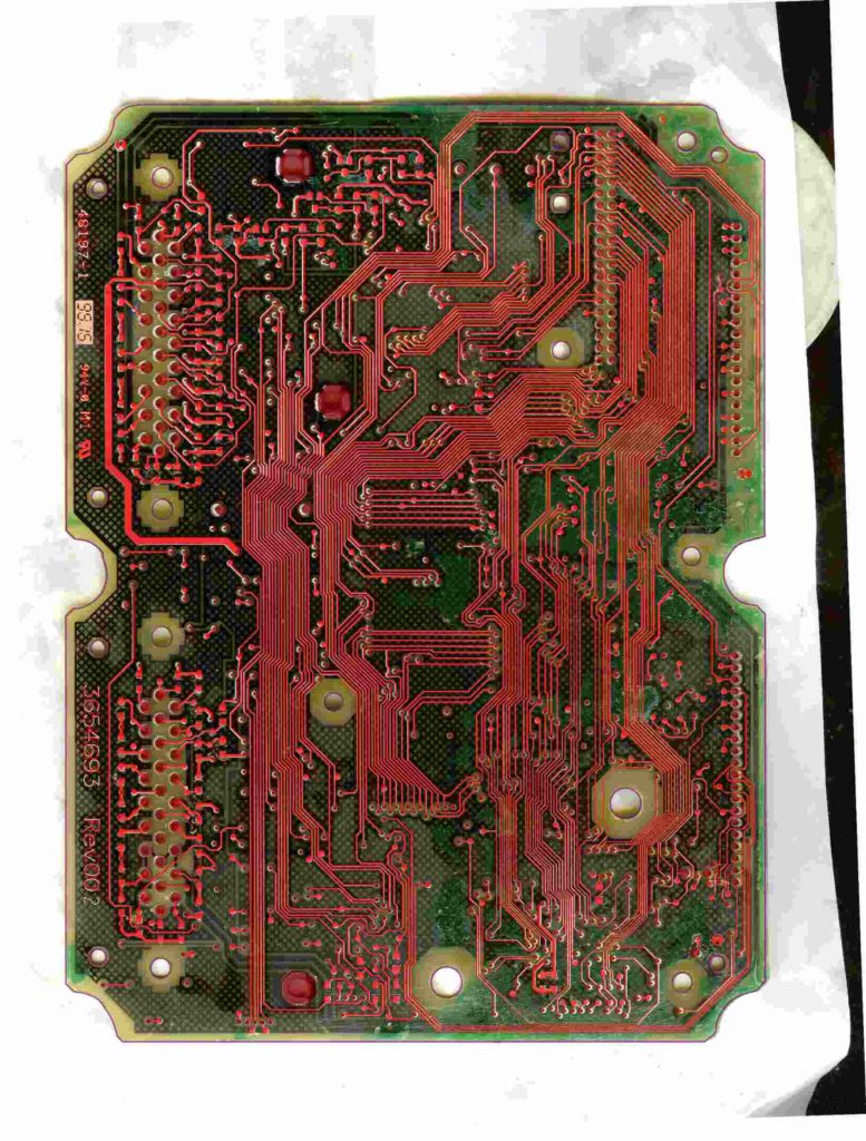
Multilayer PCB Card Cloning
Installation of multilayer PCB Card cloning, flexible arrangement must be made according to above rules when cloning, for example, for the four layers PCB plate reverse engineering, there are totally 3 solutions, optimal solution is No.1
S—-Signal layer
G—Ground layer
P—Power supply layer
SGPS/GSSP/SPGS
For solution 1, this is a main solution for most of the four layer printed circuit board reverse engineering netlist, there is a ground layer beneath the component side, critical signal will layout on the TOP layer; as for the layer thickness installation, there are below suggestion:
The core laminate for the PCB Card which can be used to satisfy the impedance control shouldn’t be too thick, since it will help to decrease the dissipated impedance on the power supply and ground layer. Ensure the decoupling effect of the power supply layer, in order to meet the shielding effect, someone has ever tried to place the ground and power supply layers on the TOP and BOTTOM layer which is the solution No.2, and there could be defects in below aspects:
1 the distance between the power supply and ground layer is too big to undertake the impedance on the power supply layer;
2 power supply and ground layer could be crack down into different part without completeness due to the soldering pad of electronic components;
3 inconsistent of signal impedance due to the incomplete reference layer;
As a matter of fact, due to the massive application of surface mount technology, in the scenario of increasing component density, the power supply, ground layer in this solution won’t provide a complete reference plane when Printed wiring board cloning, and the expected shielding effect would be difficult to come into practice. The application scope of solution No.2 is limited, but for several PCB Card cloning case, it could be an optimal choice.
Tags: pcb assemble cloning,pcb board cloning,pcb card cloning,pcb cloning,pcba cloning,printed circuit board cloning,printed wiring board cloning,pwb cloning,pwba cloning