

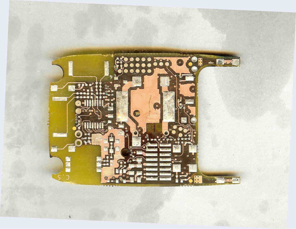
PCB Plate Reverse Engineering Mechanical Design
PCB Plate Reverse Engineering Mechanical Design is a way to extract information of printed circuit board layout scheme, gerber file and BOM, then use these informations to reproduce circuit board.
After the mechanical design, next one we need to talk about the Installation of pcb plate after reverse engineering, the mechanical support should be exist in three rims of pcb plate within one inch of its edge, according to the practical experience, if the thickness of pcb plate is around 0.031 to 0.062 inch, then the distance of its support location should be at least 4 inches;
If the thickness of pcb plate is greater than 0.093 inches, then the distance of each support pins should be at least five inches. This principle can effectively improve the pcb plate rigid capability and eliminate the syntony. And the pcb reverse engineering technology can only be determined after below items being confirmed:
1. the area on the pcb plate where doesn’t need to mount the components;
2. effect of insert and withdraw tools on the distance between two pcb plate installation;
3. design and reverse engineering fixed hole and slot in the pcb plate;
4. insert and withdraw tools must be placed in the device for usage, and their measurement must be taken into account;
5. need to use a insert and withdraw device, and normally will use screw to fix it onto the pcb plate eternally;
6. in the fixed body frame of pcb plate, and need the special design and reverse engineering on the pcb plate load bearing flange;
7. the adaptability of insert/withdraw tools with PCB Reverse Engineering dimension, shape and thickness;
Tags: duplicate circuit board,duplicate circuit card,duplicate pcb,duplicate pcb assemble,duplicate pcb board,duplicate pcb card,duplicate pcba,duplicate printed circuit board,duplicate printed wiring board,duplicate pwb,duplicate pwba