

How to Analyze and Understanding the Design and Layout of a PCB?
Analyzing and understanding the design and layout of a PCB involves a systematic approach that combines observation, documentation, and testing. Here’s a step-by-step guide:
1. Visual Inspection:
- Identify Components: Start by identifying all components on the PCB. Note down their part numbers, markings, and positions.
- Trace Routing: Follow the traces (conductive pathways) on the board to understand how components are connected.
- Layer Analysis: If the PCB has multiple layers, try to determine the layer stack-up by observing via-holes and vias.
2. Documentation:
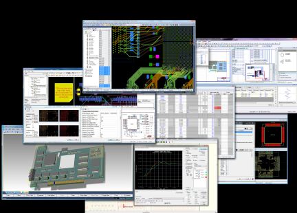
- Take Photos: Capture high-resolution images of both sides of the PCB. These visuals will be helpful during analysis.
- Make Notes: Record your observations, including component placements, markings, and any unique features.
- Create a Rough Sketch: Draw a rough schematic of the PCB layout, indicating the components and their connections as you understand them.
3. Component Datasheets and Identification:
- Gather Datasheets: Collect datasheets for the identified components. These datasheets contain crucial information about the components’ electrical characteristics.
- Identify Functionality: Understand the role of each component by referencing its datasheet and researching its function in the circuit.
4. Circuit Tracing:
- Use a Multimeter: Set the multimeter to continuity mode to trace connections between components, confirming your observations.
- Follow Traces: Trace the connections on the PCB using a multimeter to verify your initial understanding of the circuit layout.
5. Reverse Engineering Software:
- PCB Design Software: Use PCB design software (e.g., Altium Designer, Eagle, KiCad) to create a digital representation of the PCB layout. Input your observations and create a schematic based on the traced connections.
6. Functional Testing:
- Power Up the PCB: If possible and safe, power up the PCB to observe its behavior. Be cautious and ensure proper safety measures are taken.
- Probe Connections: Use oscilloscopes or logic analyzers to further understand signal paths and verify functionality.
7. Iterative Process:
- Refinement: Refine your understanding by cross-checking observations and testing results.
- Documentation Updates: Continuously update your documentation and digital representations as you gain a better understanding.
8. Seek Help:
- Online Communities/Forums: Seek advice and guidance from online communities or forums dedicated to electronics and PCB design. Others might have insights or experiences that could aid your analysis.
Remember, PCB analysis and understanding can be a meticulous process that requires patience, attention to detail, and sometimes a multidisciplinary approach. It’s not uncommon for it to take time to fully comprehend a complex PCB design.