High Speed PCB Board Reverse Engineering
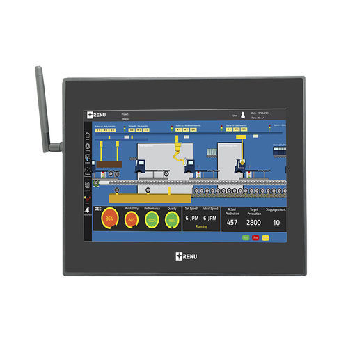
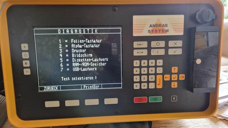
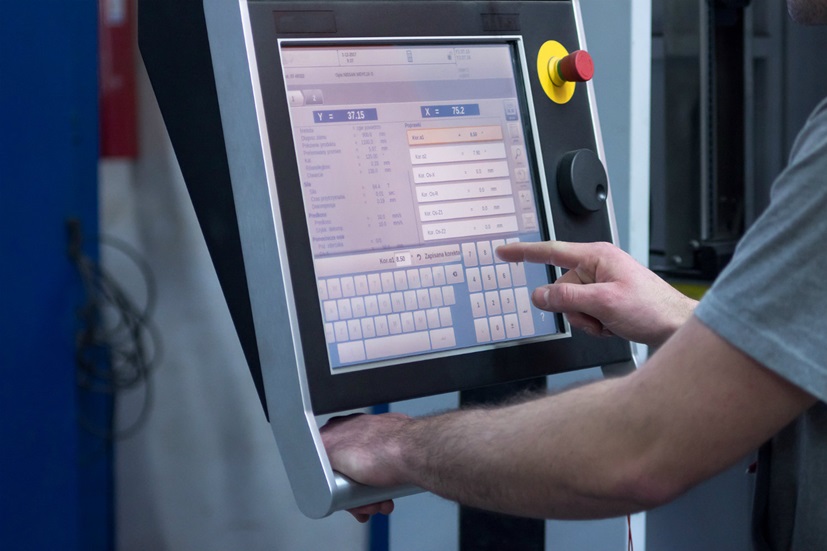
High Density Printed Circuit Board reverse engineering is increasingly important for Display and Human-Machine Interface (HMI) boards used in bulldozers, especially those driving LCD or TFT panels for operator control and real-time monitoring.
These HMI boards integrate graphics controllers, power management circuits, touch interfaces, and communication modules within compact, multilayer PCB structures. When original design data is unavailable, reverse engineering provides a practical way to recover and restore the complete electronic design, ensuring that critical display and control functions can be maintained throughout the equipment lifecycle.
High Speed PCB Board Reverse Engineering
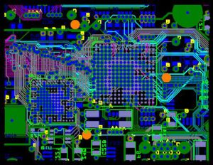
When reverse engineering PCB board, there are several issues will be existed in the process, from one side, PCB board reverse engineering need to make sure all of the components place close to each other, it can help to shorten the circuit when reverse engineering PCB board, low down the cross-talk, reflection even electro-magnetic radiation and keep the signal integrity; from other side, the spectrum generated by Radio frequency from different logic part is various too, especially in the high speed PCB board reverse engineering system, the higher the signal frequency, the radio frequency energy bandwidth generated from the digital signal jump operation is wider for PCB board reverse engineering, so in order to prevent the mutual interference among different components which has various bandwidth,
High Speed PCB board reverse engineering rules must be draw and carefully preserved, in order to solve these issues, engineers have to divide PCB Board according to different functional block, which means separate the PCB board physically by different functional sub-system. Different PCB board Reverse Engineering will apply different separation methods, can normally apply the multiple PCB board, part isolation and Layout, etc. appropriate separation on the PCB board reverse engineering can help to optimize the signal quality, simply the layout, and low down the interference. Engineer should be aware of which part belongs to what block when reverse engineering PCB board and these information can be obtained from part vendors.
Functional separation can be viewed as the separation of one functional block from another, in order to separate the circuit with different functions when reverse engineering PCB. When reverse engineering PCB, there is one simple purpose is restrict the related electro-magnetic field from specific sub-united into the area where need them. For example, engineer hopes the electro-magnetic energy from processor area won’t convert to I/O circuit. there is electrical potential difference exist among processor and I/O circuit, as long as it exist, then there will be common model energy conversion among them, so their separation must be decoupling with high quality level.
Functionality separation will need to pay attention to two aspects: handle conversion and radiation from the Radio frequency energy. Radio frequency transmitted energy can be distributed among functionality sub-system and power supply distribution system through the signal line, PCB reverse engineering is mean to distribute the useful signals to where required it and reject those without any usage.
Make practice of reverse engineering PCB separation includes two meanings: separation and interconnection.
Separation can use moat in each layer to form the blank area without copper foil clad, Moat minimum thickness is 50mil and it is like a fosse to separate the PCB into different islands.
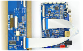
In the core technical phase, engineers perform high-density PCB reverse engineering to extract all design intelligence from the physical board. Through layer-by-layer analysis, imaging, and signal tracing, the original layout drawing and Gerber file are recreated to reflect fine-pitch routing, impedance-controlled lines, and complex via structures. At the same time, functional analysis enables restoration of the schematic diagram and netlist, accurately mapping relationships between the display driver, microcontroller, memory, backlight circuit, and input interfaces. A detailed bom list is then compiled to support clone, copy, replicate, or duplicate manufacturing. In this keyword-intensive stage, reverse engineering allows the HMI PCB to be faithfully reproduced or remanufactured.
Once documentation has been fully recovered, the focus shifts to converting reverse engineering outputs into real production assets. The restored Gerber file, schematic diagram, layout drawing, bom list, and netlist are validated and optimized for modern PCB fabrication and assembly processes. Engineers may choose to redesign or redevelop selected sections to replace obsolete LCD controllers, improve EMC performance, or enhance backlight power efficiency, while preserving original operator interface logic. This approach supports refurbish programs and enables reliable reproduce or duplicate production of HMI boards for bulldozer fleets operating in harsh environments.
Despite its advantages, high-density PCB reverse engineering of HMI boards presents notable challenges. Dense component placement, high-speed display signals, mixed-voltage domains, and sensitivity to noise can complicate the restore and recreate process. Any deviation during copy or redesign may affect display stability or operator responsiveness. However, with disciplined reverse engineering methods, these risks can be controlled. Ultimately, this technology provides a cost-effective solution to recover, remanufacture, and extend the service life of bulldozer HMI systems, supporting long-term operation, localized manufacturing, and continuous improvement of operator control and monitoring interfaces.