"Everything we build starts with design engineering. CECL manufactured boards for one of our products. It went perfectly – a real success.It is really an high quality service they have provided to us!"
By Nile Smith from Sinotech Inc.
“We had several very old device with obsolete boards need to be replaced –through CECL professional service.We got what we needed, and we’ve been using the results of the work without any problem till now.”
By Richard Anderson from TWP system Inc.
"Guys from CECL manufacture PCBs we use in one of our products, a clinometer and we’ve never had a problem with anything. The boards come in, they work. And, their team is very responsive."
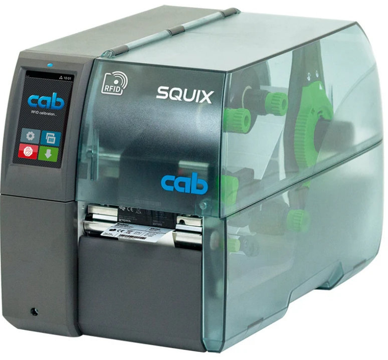
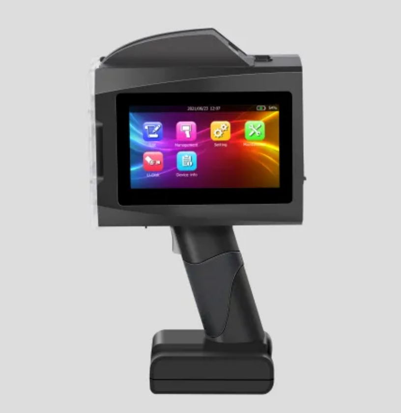
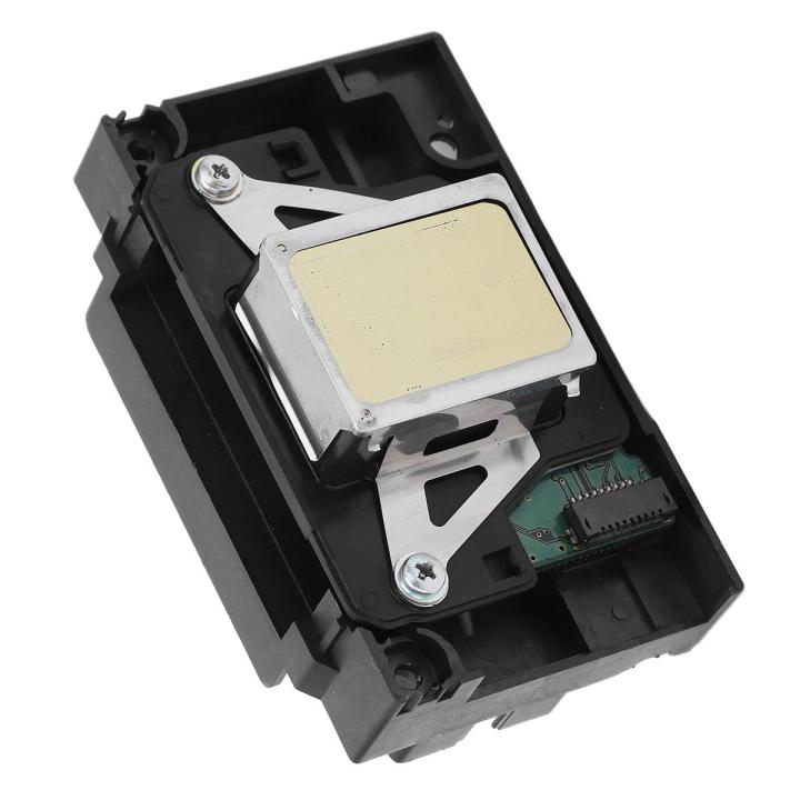
High Sensitivity Printer PCB Plate Cloning has become a vital engineering technique for industries that rely on precision printing equipment. As these printers age or their controller boards become unavailable, engineers often turn to reverse engineering to recover, reproduce, and remanufacture the circuit boards that manage print head actuation, sensor feedback, paper transport, and calibration routines. The goal is to recreate a stable, reliable controller board while maintaining full compatibility with the printer’s original functions.
La clonación de placas de circuito impreso (PCB) para impresoras de alta sensibilidad se ha convertido en una técnica de ingeniería esencial para las industrias que dependen de equipos de impresión de precisión. A medida que estas impresoras envejecen o sus placas controladoras dejan de estar disponibles, los ingenieros suelen recurrir a la ingeniería inversa para recuperar, reproducir y remanufacturar las placas de circuito que gestionan la actuación del cabezal de impresión, la retroalimentación de los sensores, el transporte de papel y las rutinas de calibración. El objetivo es recrear una placa controladora estable y fiable, manteniendo la compatibilidad total con las funciones originales de la impresora. El proceso comienza con el desmontaje de la impresora de alta sensibilidad para acceder a su placa de circuito impreso de control. Los ingenieros fotografían cada ángulo, anotan la posición de los conectores y analizan las rutas de señal. Mediante microscopios y escáneres especializados, extraen el trazado del cobre, las estructuras de vías y los detalles de la pila de capas. Esta información se digitaliza en un archivo Gerber completo, un plano de diseño y una lista de conexiones, lo que permite restaurar y copiar la placa con precisión. Durante esta etapa, también se reconstruye el diagrama esquemático para mostrar las relaciones funcionales entre los circuitos integrados, los circuitos analógicos, los módulos de control y las etapas de potencia.
The process begins with dismantling the high sensitivity printer to access its control PCB plate. Engineers photograph each angle, note connector positions, and analyze signal paths. Using specialized microscopes and scanning tools, they extract copper routing, via structures, and layer stack details. This information is then digitized into a complete Gerber file, layout drawing, and netlist, allowing the board to be restored and copied accurately. During this stage, the schematic diagram is also rebuilt to show functional relationships between the ICs, analog circuits, driver modules, and power stages.
After you get started of your High Sensitivity Printer PCB Plate Cloning project with us, all the necessary files will be submited in below format through which your High Sensitivity Printer PCB plate can be manufacture and assembly anywhere in the world, we can ensure the accuracy of your data by means of prototype running.
A clonagem de placas de circuito impresso (PCBs) de impressoras de alta sensibilidade tornou-se uma técnica de engenharia vital para indústrias que dependem de equipamentos de impressão de precisão. À medida que essas impressoras envelhecem ou suas placas controladoras se tornam indisponíveis, os engenheiros frequentemente recorrem à engenharia reversa para recuperar, reproduzir e remanufaturar as placas de circuito que gerenciam a atuação da cabeça de impressão, o feedback dos sensores, o transporte de papel e as rotinas de calibração. O objetivo é recriar uma placa controladora estável e confiável, mantendo total compatibilidade com as funções originais da impressora. O processo começa com a desmontagem da impressora de alta sensibilidade para acessar sua placa de circuito impresso de controle. Os engenheiros fotografam cada ângulo, anotam as posições dos conectores e analisam os caminhos de sinal. Usando microscópios especializados e ferramentas de digitalização, eles extraem o roteamento de cobre, as estruturas de vias e os detalhes da pilha de camadas. Essas informações são então digitalizadas em um arquivo Gerber completo, um desenho de layout e uma lista de conexões (netlist), permitindo que a placa seja restaurada e copiada com precisão. Durante essa etapa, o diagrama esquemático também é reconstruído para mostrar as relações funcionais entre os circuitos integrados (CIs), os circuitos analógicos, os módulos de driver e os estágios de potência.
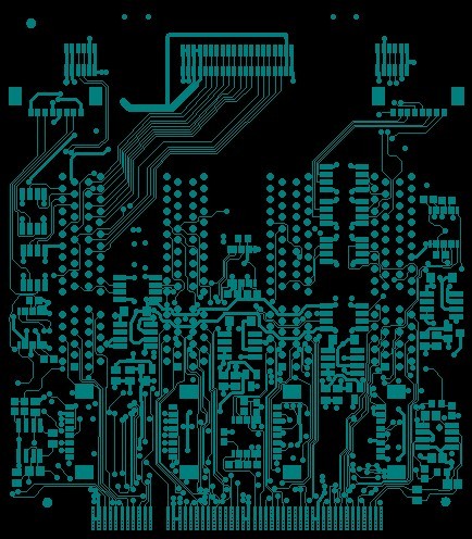
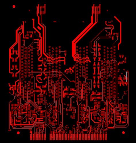
Here is sample of files and drawings you will receive, based on a typical 4 layer High Sensitivity Printer PCB Plate Cloning with components mounted on two sides:
Top layer of Gerber File from High Sensitivity Printer PCB:
Top layer of Gerber File from High Sensitivity Printer PCB
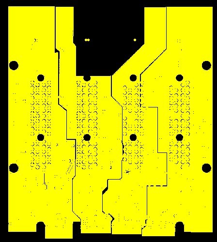
1st mid-layer of Gerber File from High Sensitivity Printer PCB Plate
2nd mid-layer of Gerber File from High Sensitivity Printer PCB Plate:
1st mid-layer of Gerber File from High Sensitivity Printer PCB Plate
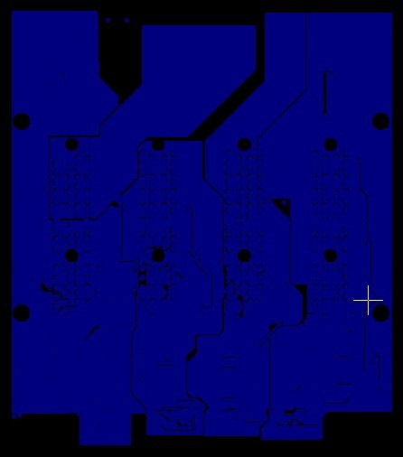
Bottom layer of Gerber File from High Sensitivity Printer PCB Plate:
1st mid-layer of Gerber File from High Sensitivity Printer PCB Plate
After the electronic structure is fully recreated, the next task is generating a precise BOM list. Each component is identified, its value confirmed, and its package measured. When part numbers are obsolete or unclear, engineers may need to redesign or redevelop certain sections to ensure that modern equivalents behave identically. In more complex cases, circuit blocks require refurbishment or functional duplication to match the timing and sensitivity of the original printer.
Le clonage de cartes PCB pour imprimantes haute sensibilité est devenu une technique d’ingénierie essentielle pour les industries qui dépendent d’équipements d’impression de précision. Lorsque ces imprimantes vieillissent ou que leurs cartes de contrôle deviennent indisponibles, les ingénieurs ont souvent recours à la rétro-ingénierie pour récupérer, reproduire et refabriquer les cartes de circuits imprimés qui gèrent l’actionnement de la tête d’impression, le retour d’information des capteurs, le transport du papier et les routines d’étalonnage. L’objectif est de recréer une carte de contrôle stable et fiable tout en conservant une compatibilité totale avec les fonctions d’origine de l’imprimante. Le processus commence par le démontage de l’imprimante haute sensibilité afin d’accéder à sa carte PCB de contrôle. Les ingénieurs photographient chaque angle, notent la position des connecteurs et analysent les chemins de signaux. À l’aide de microscopes et d’outils de numérisation spécialisés, ils extraient le routage du cuivre, les structures de vias et les détails de l’empilement des couches. Ces informations sont ensuite numérisées dans un fichier Gerber complet, un schéma d’implantation et une netlist, permettant ainsi de restaurer et de copier la carte avec précision. Au cours de cette étape, le schéma électrique est également reconstruit pour illustrer les relations fonctionnelles entre les circuits intégrés, les circuits analogiques, les modules de commande et les étages d’alimentation.
When the digital documentation is complete, it must be converted into realistic production data. This involves verifying spacing rules, checking impedance control lines, reviewing the netlist for mismatches, and confirming that all Gerber layers align perfectly. Once approved, the PCB manufacturer begins producing the bare board through lamination, drilling, plating, solder mask application, and surface finishing. Every detail must replicate the original board’s design tolerance to ensure the high sensitivity printer operates with the same precision.
Next comes component procurement. Using the BOM list, technicians source all resistors, capacitors, MOSFETs, microcontrollers, sensors, and connectors. Where older components are unavailable, the engineering team may choose to reproduce functionally-compatible parts or redesign circuits around newer technology. After procurement, assembly proceeds through automated and manual soldering processes, with high attention to thermal profiles to avoid damaging sensitive ICs. Once assembled, the cloned PCB is tested using schematic diagram references, injection of diagnostic signals, and functional comparison with the original board.
Turning reverse-engineered documents into production requires strict discipline. Any error in the Gerber file alignment, BOM interpretation, or layout reconstruction can result in noise issues, printing inaccuracies, or unstable sensor readings. Attention must be paid to grounding, shielding, trace width control, and power distribution—especially because high sensitivity printers rely heavily on clean analog signals and noise-free feedback loops.
La clonazione della piastra PCB per stampanti ad alta sensibilità è diventata una tecnica ingegneristica fondamentale per le industrie che si affidano a apparecchiature di stampa di precisione. Con l’invecchiamento di queste stampanti o la mancata reperibilità delle schede controller, gli ingegneri spesso ricorrono al reverse engineering per recuperare, riprodurre e rifabbricare le schede che gestiscono l’attuazione della testina di stampa, il feedback dei sensori, il trasporto della carta e le routine di calibrazione. L’obiettivo è ricreare una scheda controller stabile e affidabile, mantenendo al contempo la piena compatibilità con le funzioni originali della stampante. Il processo inizia con lo smontaggio della stampante ad alta sensibilità per accedere alla piastra PCB di controllo. Gli ingegneri fotografano ogni angolazione, annotano le posizioni dei connettori e analizzano i percorsi dei segnali. Utilizzando microscopi e strumenti di scansione specializzati, estraggono i dettagli del routing in rame, delle strutture dei via e degli stack di strati. Queste informazioni vengono quindi digitalizzate in un file Gerber completo, in un disegno di layout e in una netlist, consentendo il ripristino e la copia accurata della scheda. Durante questa fase, viene anche ricostruito lo schema elettrico per mostrare le relazioni funzionali tra i circuiti integrati, i circuiti analogici, i moduli driver e gli stadi di potenza.
Although challenges such as multi-layer de-tracing, masked vias, resin-filled holes, or coated surfaces may slow the process, successful PCB plate cloning significantly extends the life of high sensitivity printers. It provides a cost-effective way to replicate, clone, and remanufacture rare boards while preserving the precision performance these printers are known for.
Circuit Engineering Company Limited provide a complete PCB Reverse Engineering, PCB Clone and PCB Restoration service, Rapid Prototyping and functional test services using the latest technologies combined with traditional skills for a wide range of industries. By integrating our traditional skills with the latest technologies, we can offer clients a comprehensive portfolio of product development services all under one roof. For more details please contact our customer service team.