

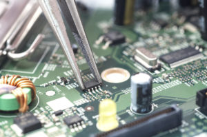
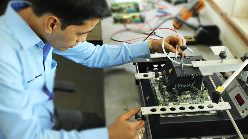
Electronic PCB Card Reverse Engineering Process
The post stage of electronic pcb card reverse engineering process must also be able to provide a authentication functions which is dedicated on the high speed design. In the past, circuit design engineer will do the post verification after layout and pcb board reverse engineering when there is key network on the PCB, and comprehensive authentication for the whole Electronic PCB Card will be viewed as complicate and time consuming.

However, this viewpoint is being changed, since in the high speed circuit board reverse engineering process, the interaction among hundreds of millions of networks are very difficult to predict. and in order to assure the reliability of the design and Electronic pcb card reverse engineering, the only way is comprehensive simulation on the layout.
An ideal high speed PCB reverse engineering must be able to solve these issues, and the design environment of this process must include high speed, high precision signal analysis engine, and be able to complete all of the signal simulation process in the electronic pcb card which has been reversed engineering in a related short period of time.
Meanwhile, the simulation engineer must be able to simulate several electronic pcb cards and multiple devices, to better support the multiple electronic pcb card reverse engineering database in the design environment.
Tags: reverse engineering electronic pcb card artwork,reverse engineering electronic pcb card bom,reverse engineering electronic pcb card design,reverse engineering electronic pcb card diagram,reverse engineering electronic pcb card gerber file,reverse engineering electronic pcb card layout,reverse engineering electronic pcb card schematic