Copy Electric Drill PCB Board Trace
Copy Electric Drill PCB Board Trace and the placement of power, ground and signal traces properly is a top subject to be discussed in this articles; After cloning pcb board components’ placement drawing, power, ground, and signal traces can be placed next to ensure your signals have clean and trouble-free paths of travel. Here are some guidelines to keep in mind at this stage of reverse engineering printed circuit board process:
1, Locate the power and ground plane layers in the process of reverse design
It is always recommended to place the power and ground plane layers inside the pcb circuit board while keeping them symmetrical and centered. This helps prevent your pcb board from warping, which is also a matter of properly positioning your components. For powering the ICs, it is recommended to use common channels for each supply, ensure a solid and consistent trace width, and avoid daisy-chaining power connections from component to component.
2, Signal line wiring connection
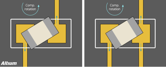
Next, connect the signal lines according to the printed circuit board copying situation in the schematic diagram. It is recommended to always take the shortest possible paths and direct path routing between components. If your components need to be fixed in the horizontal direction without any deviation, it is recommended that the components on the circuit board be routed basically horizontally, and then vertically routed after the components are routed out.
In this way, as the solder migrates during soldering, the components will be fixed in the horizontal direction. This is shown in the top half of the figure below. The signal routing method in the lower part of the figure below may cause component deflection as the solder flows during soldering.
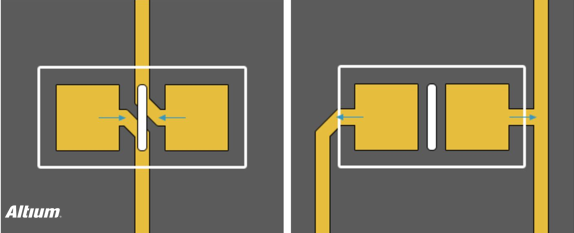
GOOD