

Printed Circuit Board Ground Plane Reverse Design
The ground plane of Printed circuit board can act as a shield where sensitive signals cross. Printed Circuit Board Ground Plane Reverse Design can help to extract PCB board ground layer drawing out from original PCB card, Below Figure shows a good layout for a data acquisition board where all sensitive areas are isolated from each other and signal paths are kept as short as possible.
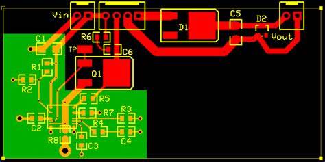
While real life is rarely as simple as this, the principle remains a valid one.
In the process of reverse design PCB Ground Plane, there are a number of important points to be considered when making signal and power connections.
First of all a connector is one of the few places in the system where all signal conductors must run in parallel—it is therefore imperative to separate them with ground pins (creating a Faraday shield) to reduce coupling between them.
Multiple ground pins are important for another reason: they keep down the ground impedance at the junction between the board and the backplane. The contact resistance of a single pin of a PCB connector is quite low (typically on the order of 10 mÙ) when the board is new—as the board gets older the contact resistance is likely to rise, and the board’s performance may be compromised.
It is therefore well worthwhile to allocate extra PCB connector pins so that there are many ground connections (perhaps 30% to 40% of all the pins on the PCB connector should be ground pins). For similar reasons there should be several pins for each power connection.