

PCB Reverse Engineering Hardware
Key Hardware Tools for PCB Reverse Engineering
- High-Resolution Imaging Systems
- Microscopes and Cameras: High-magnification microscopes and digital cameras are essential for inspecting PCB layers, tracing copper traces, and identifying component placements. Advanced systems can capture multi-layer board structures, even for complex designs.
- X-ray Imaging: For multi-layer PCBs, X-ray systems enable non-destructive inspection of internal layers, vias, and buried components, revealing hidden connections that are invisible to optical tools.
- Electrical Testing Equipment
- Oscilloscopes and Multimeters: These tools measure electrical properties such as voltage, resistance, and signal integrity, helping engineers map out circuit functionality and validate cloned designs.
- Network Analyzers: Used for impedance testing and signal path analysis, critical for high-speed PCB designs where trace geometry affects performance.
- 3D Scanners and Coordinate Measuring Machines (CMM)
- These devices create precise digital models of PCBs by scanning physical dimensions, component heights, and pad locations. They ensure accurate replication of board layouts, especially for dense or irregularly shaped designs.
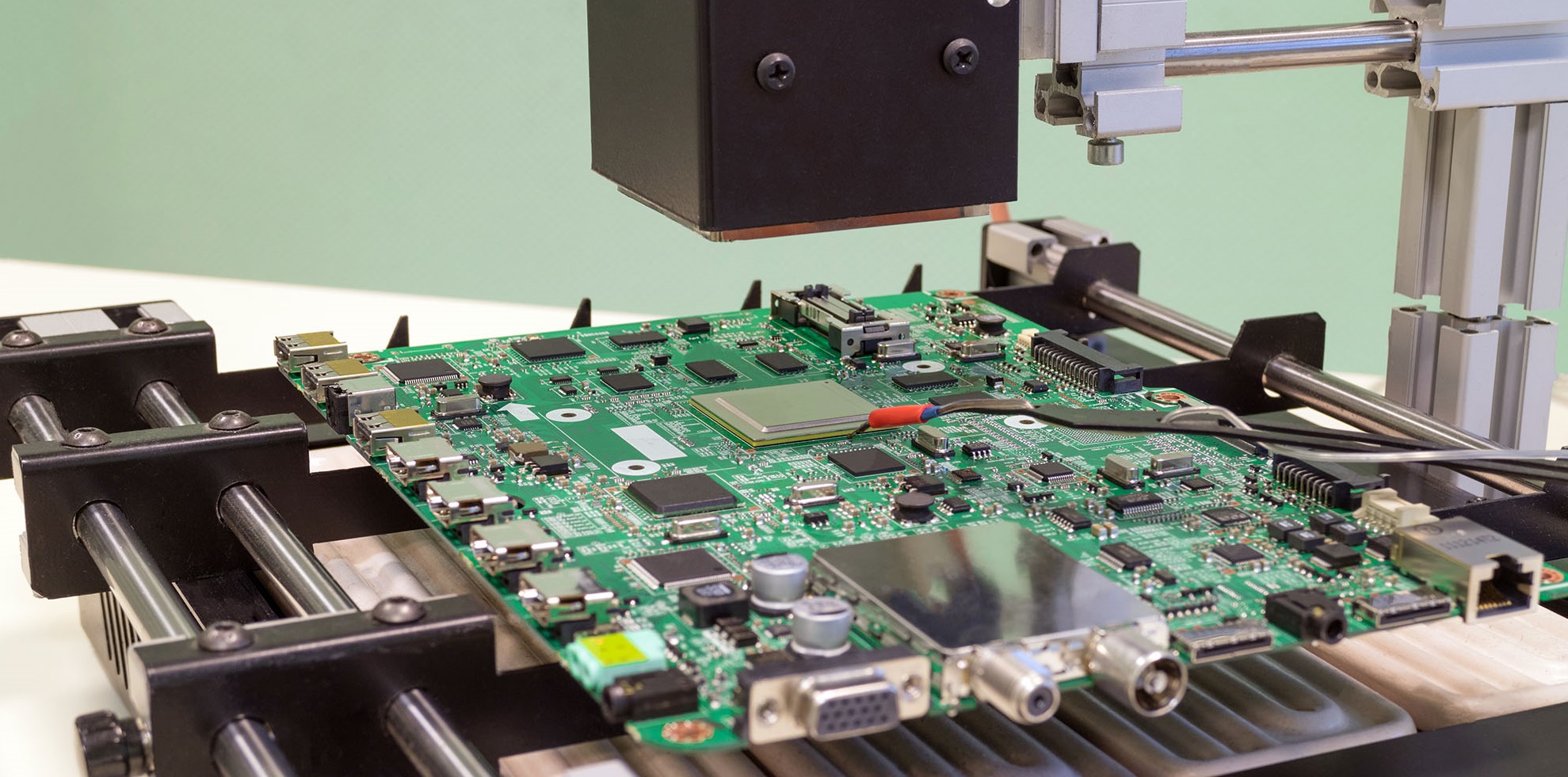
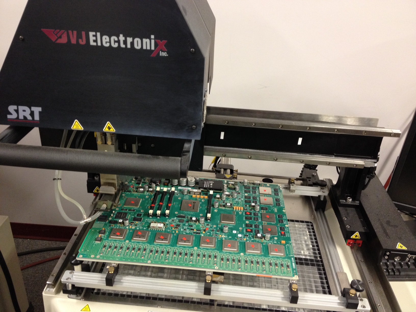
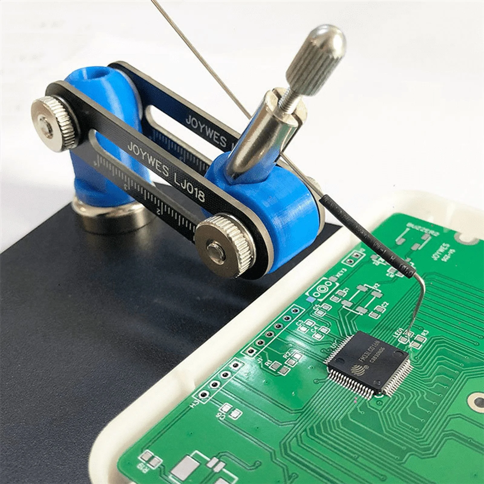
- Desoldering and Probing Tools
- Hot Air Rework Stations: Allow safe removal of components for analysis without damaging the PCB.
- Microprobes: Used to test individual traces or pins, aiding in signal tracing and debugging.
- Semiconductor Decapsulation Tools
- Chemical or laser-based decapsulators expose integrated circuit (IC) dies for analysis, enabling engineers to reverse engineer firmware or proprietary chip designs.
Unique Techniques in PCB Cloning
- Layer-by-Layer Deconstruction
- For multi-layer boards, engineers sequentially remove layers (e.g., through grinding or chemical etching) to scan each one. Advanced software like CBR5.3 then reconstructs the board’s layout from these scans, supporting up to 30 layers and Protel compatibility.
- Signal Tracing and Netlist Generation
- By probing traces and using automated tools, engineers generate a netlist (a map of electrical connections). Software like P2S converts PCB layouts into schematic diagrams, streamlining the cloning process.
- Component Reverse Engineering
- Techniques like wire bonding analysis (e.g., identifying gold vs. aluminum bonds) and ball grid array (BGA) rework are critical for replicating IC packaging. Thermal ultrasound bonding, for instance, is commonly used to study chip interconnects.
- Impedance and EMI Mitigation
- Cloning high-speed PCBs requires adherence to design rules like the 3W principle (trace spacing) and 20H rule (ground plane indentation) to minimize crosstalk and electromagnetic interference.
- Validation via Simulation
- Tools like PowerSI and Clarity 3D simulate signal integrity and thermal performance, ensuring the cloned PCB matches the original’s electrical behavior.
Ethical and Legal Considerations
Conclusion
PCB reverse engineering combines advanced hardware—such as imaging systems, electrical testers, and 3D scanners—with meticulous techniques like layer deconstruction and signal tracing. While powerful, these tools require expertise to navigate technical and legal challenges. As technology evolves, innovations like biodegradable PCBs and AI-driven analysis may further transform this field, enabling faster and more sustainable reverse engineering solutions.
For further details, refer to specialized tools like CBR5.3 or explore industry standards in signal integrity.
PCB Reverse Engineering Hardware should be examined against the unrestricted technical documentation available, such as manuals, drawings, specifications, etc., to ensure the hardware is accurately reflected by the documentation.
The hardware applied for PCB reverse engineering should be compared for uniformity of components, particularly fabricated parts. In the event that discrepancies or inconsistencies are discovered, the hardware should take precedence over the existing documentation for PCB reverse engineering purposes, and all discrepancies should be reported to the cognizant command.
Often electronic assemblies will use components of a higher reliability class and a decision will be required on which takes precedence, the hardware or the existing documentation. This should be done by the project engineer familiar with the initial testing of the item during the acquisition cycle.