

Reverse Engineering Printed Circuit Board Service
Reverse Engineering Printed Circuit Board Service can help engineer restore the schematic diagram, gerber file and layout drawing from physical PCB board;
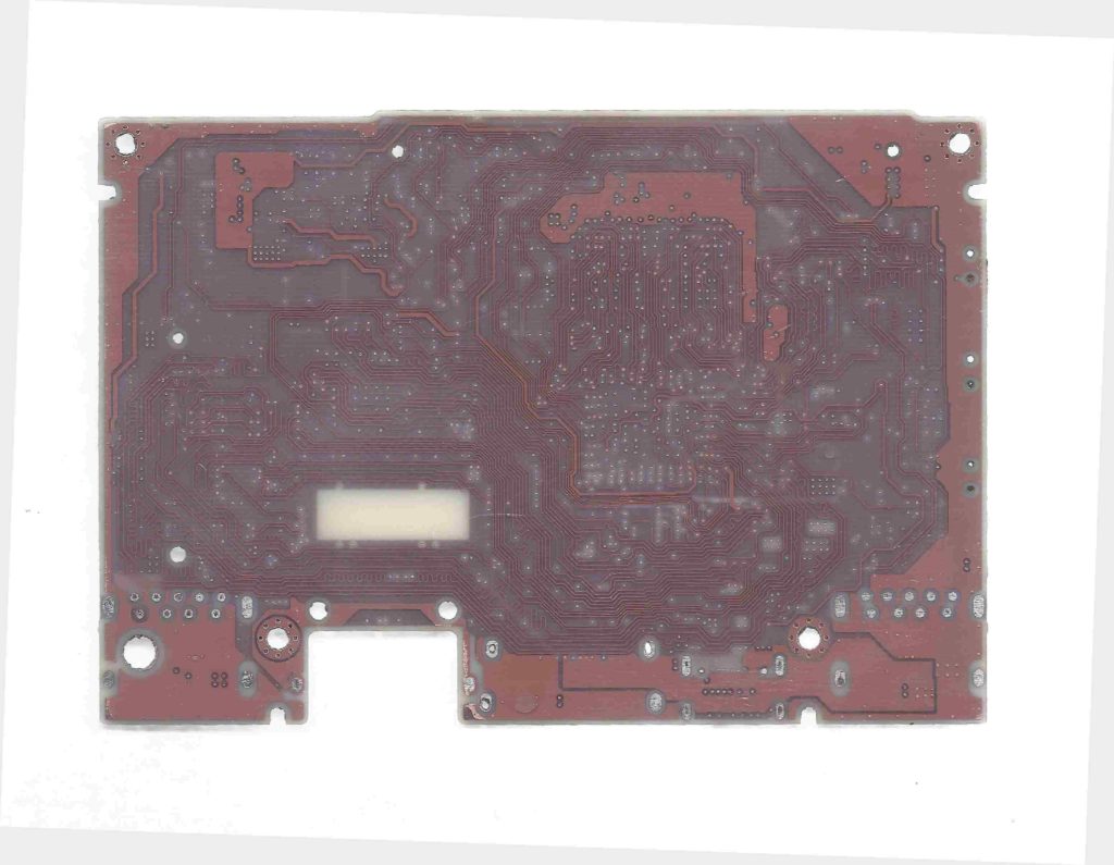
Reverse engineering printed circuit board Service has been widely applied on a great variety of industry, as we all know, it still one of the most prevail and normally use Assembly technology in the PCB board manufacture: through hole design technology. So in the process of cloning printed wiring board, we still have a lot of chances to see and need to get used to this kind of technology:
Through hole PCB board producibility design in the process of reverse engineering PRINTED CIRCUIT BOARD:
As for the electronic products, the producibility of it after reverse engineering PRINTED CIRCUIT BOARD for the reverse engineer is critical, which is also known as DESIGN FOR MANUFACTURE, if PRINTED CIRCUIT BOARD design and layout can’t match the DESIGN FOR MANUFACTURE requirement, it will greatly decrease the production efficiency of electronic PCB production.
In the worse situation, even the PCB board can’t be produced if PCB board design or layout. Nowadays, through hole technology still account for great share of PCB board manufacture market, DESIGN FOR MANUFACTURE concept can play a very effective role in the aspect of through hole PCB manufacturing efficiency and reliability, DESIGN FOR MANUFACTURE can also help to bring down the cost of through hole PCB board manufacturer flaw and keep the competitive edge.
Hereby we would like to introduce some of the DESIGN FOR MANUFACTURE methods use on the through hole. All of these methods has universal application manufacturing principally, but we can’t ensure it is applicable to all of the situations. However, as for those design or layout PCB board engineers for the printed wiring card reverse engineering service, it is believed the useful effect.
Tags: reverse engineering circuit board,reverse engineering circuit card,reverse engineering pcb,reverse engineering pcb assemble,reverse engineering pcb board,reverse engineering pcb card,reverse engineering pcba,reverse engineering printed circuit board,reverse engineering printed wiring board,reverse engineering pwb,reverse engineering pwba