

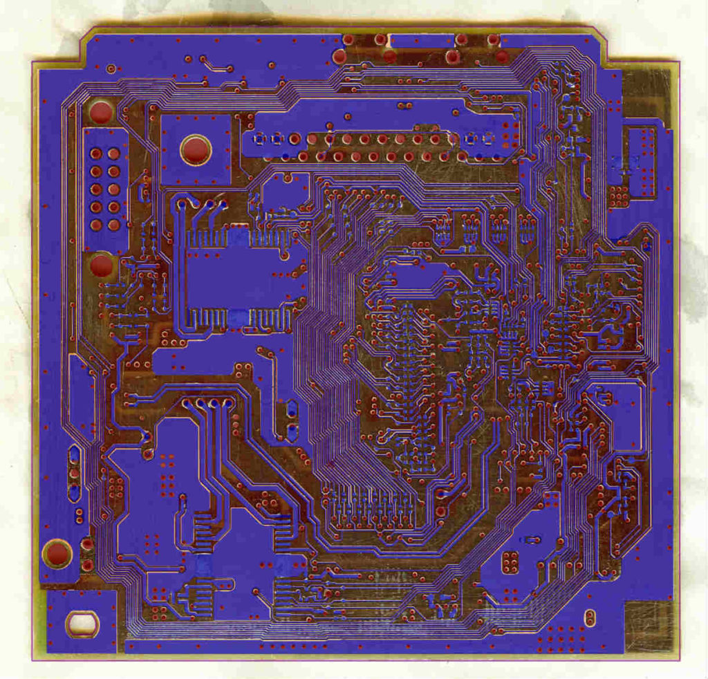
Printed Wiring Card Design Reverse Engineering Lines
Printed Wiring Card Design Reverse Engineering Lines are used to draw tracks on the pc board. When in the line mode, each Btn1 press establishes one end of a line. Once the second point is defined, the line is drawn and a new line started where the first one ended.
You can abandon the new starting point in favor of another by pressing Ctrl-Btn1, or Btn3, but don’t use Btn2. The undo function (U key or ‘undo last operation’ from the Edit menu) will take you back point by point if you use it while in the line mode.
If you drag the pointer out of the Layout area when electronic pcb board Reverse Engineering while drawing a line, the display will auto-scroll (assuming sufficient zoom for scrolling). To stop auto-scroll, simply pass the pointer over the panner control.
You can swap which side of the board you are viewing by pressing the Tab key, or by selecting ‘view solder side’ from the Screen menu. The layer groups just have a name or number associated with them – where they are sandwiched in the board is left for you to tell the manufacturer.
The silkscreen layer from copying Printed wiring card gerber file is special because there are actually two silkscreen layers, one for the top (component) and one for the bottom (solder) side of the board.
Which silk layer you draw on is determined by the side of the board that you are viewing. If you are viewing the component side, then drawing on the silk layer draws to the component-side silk layer.
The netlist layer is another special layer. It shows rat’s-nest lines (i.e. guides that show how the netlist expects the element to interconnect). If you make this the active layer, you can use the Line tool to add entries into the netlist, or to delete connections from the netlist window.
Except for these two purposes, you should not make the netlist layer the active layer. Usually there is no need to do this because a separate schematic package should be used to create the netlist. Printed wiring card cloning can automatically draw all of the rats from the netlist. In some cases you may want to make a small change without going to the trouble of modifying the schematic, which is why this facility is provided.
Tags: duplicate printed wiring card artwork,duplicate printed wiring card bom,duplicate printed wiring card component list,duplicate printed wiring card design,duplicate printed wiring card diagram,duplicate printed wiring card documents,duplicate printed wiring card drawing,duplicate printed wiring card gerber file,duplicate printed wiring card layout,duplicate printed wiring card part list,duplicate printed wiring card schematic