

Printed Circuit Board Reverse Engineering Technology
As for Printed Circuit Board Reverse Engineering Technology, many people don’t understand what’s it and simply believe PCB board reverse engineering is just replicate 100% extra same product without any changes. But on the contrary, Reverse engineering is not only a printed wiring board replication process, but a learning process. The final purpose is to learn the advanced electronic and electrical design technology from abroad and for second phase development.
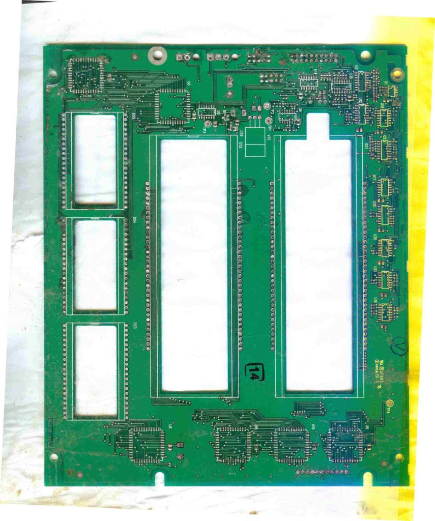
Reverse engineering is a PCB board reverse design research process, through which a PCB’s design circuit schematic can be obtained as well as the layout and bill of material.
There will be only 2-3 months required to learn other advanced technology which has been researched and developed for years through reverse engineering process. It means we can swiftly keep up the pace with other competitive marketers and this technology will sometimes make a breakthrough for the research and development team.
Meanwhile reverse engineering development can greatly increase the pace of research and development, it give the impulse to the electronic development to shorten the electronic product update cycle since reverse engineering technology low down the barrier.
Tags: pcb assemble cloning,pcb board cloning,pcb card cloning,pcb cloning,pcba cloning,printed circuit board cloning,printed wiring board cloning,pwb cloning,pwba cloning