

Printed Circuit Board Reverse Engineering Experience
Printed Circuit Board Reverse Engineering Experience can be accumulated after years of practice, the main purpose of this execution is to restore PCB board documents include schematic, circuitry scheme and gerber file.
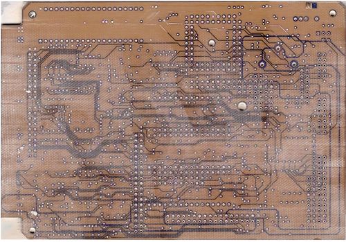
PC Board Reverse Engineering is a industry which requires sufficient experience, circuit engineering co.,ltd has been in this industry for years and have accumulated lots of experiences. We have seen printed circuit boards from over several hundreds of different products in various industries, such as air conditioning, Liquid Crystal Diode TV, digital photograph frame, and other automatic industry products, etc.
In view of a Pcb card reverse engineering engineers, some of these circuit boards have good design features, some others not. The only standard for design a good PRINTED CIRCUIT BOARD is whether it can be checked and viewed by engineers from manufacturing factory clearly and effortlessly, without any misunderstanding which can cause the wrong operation and production.
Below we introduce several aspects about PCB board layout design, design solder resist mask, and the most commonly see problems in the solder resist design is copper exposure on some of the copper area or circuit tracks. For example, on some of the copper pad need to have solder resist opening for the thermal dissipation.
Or expose copper on some of the tracks with great current go through, so in the process of PCB Reverse Engineering, engineers will add an extra solder resist layer, or place on the mechanic layer, or on the track layer etc and without any specified description. According to our PC board Reverse Engineering experience, solder resist pattern should be placed on the TOP SOLDERMASK or BOTTOM SOLDERMASK layer which makes people easier to understand, besides, the solder resist bridge among the IC lead should be preserved.
Tags: pcb assemble reverse engineering,pcb board reverse engineering,pcb card reverse engineering,pcb reverse engineering,pcba reverse engineering,Printed Circuit Board Reverse Engineering,printed wiring board reverse engineering,pwb reverse engineering,pwba reverse engineering