"Everything we build starts with design engineering. CECL manufactured boards for one of our products. It went perfectly – a real success.It is really an high quality service they have provided to us!"
By Nile Smith from Sinotech Inc.
“We had several very old device with obsolete boards need to be replaced –through CECL professional service.We got what we needed, and we’ve been using the results of the work without any problem till now.”
By Richard Anderson from TWP system Inc.
"Guys from CECL manufacture PCBs we use in one of our products, a clinometer and we’ve never had a problem with anything. The boards come in, they work. And, their team is very responsive."
By Ken Camerlo from Hi-END ADV Inc.
You are here: Home > Reverse Engineering PCB > Printed Circuit Board Reverse Engineering For Electro-Magnetic Compatibility
Printed Circuit Board Reverse Engineering For Electro-Magnetic Compatibility
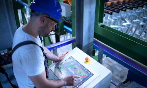
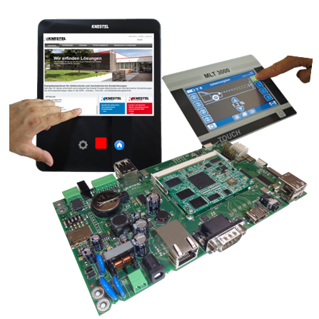
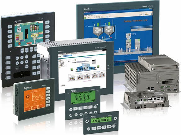
Printed Circuit Board Reverse Engineering For Electro-Magnetic Compatibility is a specialized engineering discipline widely applied to excavator Display and Human-Machine Interface (HMI) boards, including LCD and TFT panels used for operator control, diagnostics, and real-time monitoring feedback loops. These boards integrate digital processing, backlight power circuits, communication interfaces, and sensitive display drivers, making electromagnetic compatibility a core concern during any reverse engineering activity.
Der Reverse-Engineering-Prozess beginnt mit einer systematischen Untersuchung der Originalplatine, um deren ursprüngliches Design zu rekonstruieren. Ingenieure analysieren Lagenaufbauten, Abschirmungsstrukturen, Erdungsstrategien und Signaltrennung, bevor sie technische Dokumente wie Gerber-Datei, Schaltplan, Layoutzeichnung, Stückliste und Netzliste extrahieren. Mithilfe dieser Datensätze lässt sich das Originaldesign rekonstruieren und verifizieren, wobei die EMV-Konformität in den anspruchsvollen Umgebungen von Baggern gewährleistet bleibt. Nach der Rekonstruktion des Schaltplans identifizieren die Ingenieure Hochgeschwindigkeitsschnittstellen, Timing-Leitungen für die Anzeige, CAN- oder RS-485-Kommunikationswege und Spannungsregelungsschaltungen. Anschließend wird die Layoutzeichnung überarbeitet, um die Impedanzkontrolle zu gewährleisten, Übersprechen zu minimieren und elektromagnetische Störungen zu vermeiden, die die Bildschirmausgabe verfälschen oder die Bedienereingaben beeinträchtigen könnten. In dieser Phase kann die Platine geklont, kopiert oder selektiv repliziert werden, um die ursprüngliche Leistung beizubehalten und gleichzeitig Verbesserungen hinsichtlich Komponentenverfügbarkeit oder Herstellbarkeit zu ermöglichen.
The reverse engineering process starts with a systematic inspection of the original board to recover and restore its design intent. Engineers analyze layer stack-ups, shielding structures, grounding strategies, and signal segregation before extracting technical documents such as the Gerber file, schematic diagram, layout drawing, BOM list, and netlist. These data sets allow the original design to be recreated and verified while maintaining EMC compliance in electrically harsh excavator environments.
Reverse Engineering Printed circuit board need to take the electro-magnetic compability issue into consideration. Electro-magnetic compatibility means the system or device like PRINTED CIRCUIT BOARD won’t produce any electro-magnetic interference on other items in the same place when they all working in the electro-magnetic environment.
Once the schematic diagram is rebuilt, engineers identify high-speed interfaces, display timing lines, CAN or RS-485 communication paths, and power regulation circuits. The layout drawing is then redesigned to preserve impedance control, minimize crosstalk, and prevent electromagnetic interference that could distort screen output or disrupt operator inputs. At this stage, the board may be cloned, copied, or selectively replicated to match the original performance while allowing improvements for component availability or manufacturability.
Le processus de rétro-ingénierie débute par une inspection systématique de la carte d’origine afin de reconstituer et de restaurer sa conception. Les ingénieurs analysent l’empilement des couches, les structures de blindage, les stratégies de mise à la terre et la séparation des signaux avant d’extraire les documents techniques tels que le fichier Gerber, le schéma, le plan d’implantation, la nomenclature et la netlist. Ces données permettent de recréer et de vérifier la conception d’origine tout en garantissant la conformité aux normes CEM dans les environnements électriques difficiles des excavatrices. Une fois le schéma reconstitué, les ingénieurs identifient les interfaces haut débit, les lignes de synchronisation d’affichage, les chemins de communication CAN ou RS-485 et les circuits de régulation de puissance. Le plan d’implantation est ensuite repensé pour préserver le contrôle d’impédance, minimiser la diaphonie et éviter les interférences électromagnétiques susceptibles de déformer l’affichage ou de perturber les entrées opérateur. À ce stade, la carte peut être clonée, copiée ou répliquée sélectivement pour reproduire les performances d’origine tout en optimisant la disponibilité des composants ou la fabricabilité.
The purpose for electro-magnetic compatibility is not only withstand the external interference from other electronic devices to ensure the electronic device can work in the electro-magnetic environment properly, but also decrease the electro-magnetic on other device while operation.
Printed Circuit Board Reverse Engineering For Electro-Magnetic Compatibility
Accompany with the higher sensibility of electronic device, the ability to accept the minor signals become stronger and stronger, and the band width of electronic product also being widening alongside with smaller size, which require the capability to tolerate the electro-magnetic interference become stronger. The electro-magnetic wave generated by some working electronic device could have electro-magnetic interference on the surrounding device, cause malfunctions or affect the signal transmitting. Furthermore, excessive electro-magnetic interference will have electro-magnetic pollution, and damage the human body healthy, corrupt the ecology environment.
Circuit Engineering Company Limited continues to be recognized as the Southern China Leader in Services for PCB Reverse Engineering, PCB Clone, PCB Copy and PCB Replicate. With the advancement of today’s modern circuit board technology, it is more important than ever to have specialists available to help you at a moment’s notice. Circuit Engineering Company Limited have gained an excellent reputation for the reliability and speed of service with many large manufacturing organisations, throughout a diverse range of industries. We are excited about the opportunity to serve you, and assure you that we will continue to advance our knowledge, hone our skills and maintain the state-of-the-art equipment needed to provide you with the highest level of service possible.
El proceso de ingeniería inversa comienza con una inspección sistemática de la placa original para recuperar y restaurar su propósito de diseño. Los ingenieros analizan la superposición de capas, las estructuras de blindaje, las estrategias de conexión a tierra y la segregación de señales antes de extraer documentos técnicos como el archivo Gerber, el diagrama esquemático, el plano de diseño, la lista de materiales y la lista de conexiones. Estos conjuntos de datos permiten recrear y verificar el diseño original, manteniendo al mismo tiempo la conformidad con la EMC en entornos de excavadoras con altas exigencias eléctricas. Una vez reconstruido el diagrama esquemático, los ingenieros identifican las interfaces de alta velocidad, las líneas de temporización de la pantalla, las rutas de comunicación CAN o RS-485 y los circuitos de regulación de potencia. El plano de diseño se rediseña entonces para preservar el control de impedancia, minimizar la diafonía y evitar interferencias electromagnéticas que podrían distorsionar la salida de la pantalla o interrumpir las entradas del operador. En esta etapa, la placa puede clonarse, copiarse o replicarse selectivamente para igualar el rendimiento original, permitiendo al mismo tiempo mejoras en la disponibilidad o la capacidad de fabricación de los componentes.
Assembly of the new PCB requires strict adherence to grounding zones, shielding placement, and signal routing. Improper assembly can introduce noise into display panels or cause unstable touch or button responses. After assembly, functional and EMC validation ensures that the reverse-engineered board performs reliably in real excavator cabins.
Converting restored documents into production requires careful redevelopment planning. Manufacturing tolerances, component substitutions, and assembly processes must all be reviewed to avoid EMC degradation. The technique is widely used to support legacy equipment, extend product life cycles, and enable maintenance of discontinued HMI systems.
Il processo di reverse engineering inizia con un’ispezione sistematica della scheda originale per recuperarne e ripristinarne l’intento progettuale. Gli ingegneri analizzano la disposizione degli strati, le strutture di schermatura, le strategie di messa a terra e la segregazione dei segnali prima di estrarre documenti tecnici come il file Gerber, lo schema elettrico, il disegno del layout, la distinta base e la netlist. Questi set di dati consentono di ricreare e verificare il progetto originale, mantenendo al contempo la conformità EMC in ambienti di escavazione elettricamente difficili. Una volta ricostruito lo schema elettrico, gli ingegneri identificano le interfacce ad alta velocità, le linee di temporizzazione del display, i percorsi di comunicazione CAN o RS-485 e i circuiti di regolazione della potenza. Il disegno del layout viene quindi riprogettato per preservare il controllo dell’impedenza, ridurre al minimo la diafonia e prevenire interferenze elettromagnetiche che potrebbero distorcere l’output dello schermo o interrompere gli input dell’operatore. In questa fase, la scheda può essere clonata, copiata o replicata selettivamente per riprodurre le prestazioni originali, consentendo al contempo di migliorare la disponibilità o la producibilità dei componenti.
Difficulties often arise from multilayer boards, mixed-signal regions, or proprietary display interfaces. However, with disciplined reverse engineering and EMC-focused validation, companies can confidently duplicate, reproduce, and deploy reliable HMI PCB solutions for heavy machinery applications.