

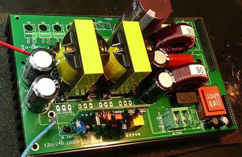
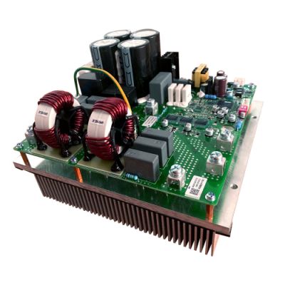
Reverse Engineering Power Inverter Circuit Board Design File
Reverse Engineering Power Inverter Circuit Board Design File needs to pay attention to below 3 points:
1, Required DUT, connector/receptacle or other mechanical component’s orientation;
On which side of the Power Inverter Circuit Board are critical components located? These requirements are missed a lot in the input package. But if design engineers don’t have the relevant information, it can stall the progress of cloning Power Inverter Circuit Board Design File. Also, if no orientation requirements are given for the desired device, the design engineer may assume that the orientation is at his discretion. Changing the orientation of a device after the recreation of printed circuit board layout design is complete can be disastrous to the layout design! If the device does not have orientation requirements, it is best to specify it up front, which will avoid many problems.
2, Electrical Circuitry Functions;
It is impossible for a design engineer to understand your signal performance requirements just by looking at a schematic. You communicate desired performance and signal characteristics to design engineers regarding high-speed data rates pcb board reverse engineering, impedance control, phase matching, and differential pair coupling. Attention should be paid to the current/voltage of the power supply. After evaluation and discussion with the design engineer, it may be determined that a circuit simulation test simulation experiment should be performed to ensure the best results.
3, Pritned Circuit Board Shape, Profile or Dimension;
Make sure that the input package contains detailed requirements for the desired power inverter pc board shape or form factor. For automatic test equipment (ATE) testing, which manufacturer’s tester and tester model will the board be used in? What is this tester configuration? Layout engineers need to verify that the analysis of pcb board dimension meets requirements and that their location on the board matches that of the tester. Make sure that the appropriate layout on the board corresponds to the location of the mechanism or connector that secures the interface.