"Everything we build starts with design engineering. CECL manufactured boards for one of our products. It went perfectly – a real success.It is really an high quality service they have provided to us!"
By Nile Smith from Sinotech Inc.
“We had several very old device with obsolete boards need to be replaced –through CECL professional service.We got what we needed, and we’ve been using the results of the work without any problem till now.”
By Richard Anderson from TWP system Inc.
"Guys from CECL manufacture PCBs we use in one of our products, a clinometer and we’ve never had a problem with anything. The boards come in, they work. And, their team is very responsive."
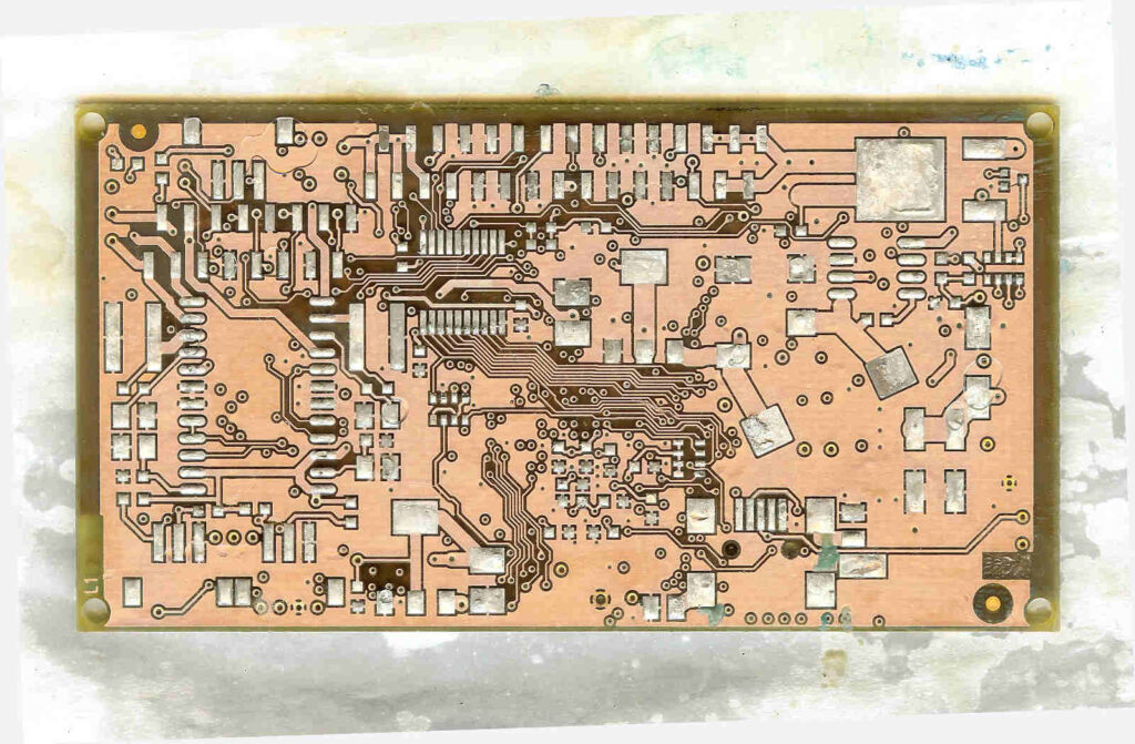
PCB Reverse Engineering for Side Road and Decoupling
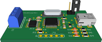
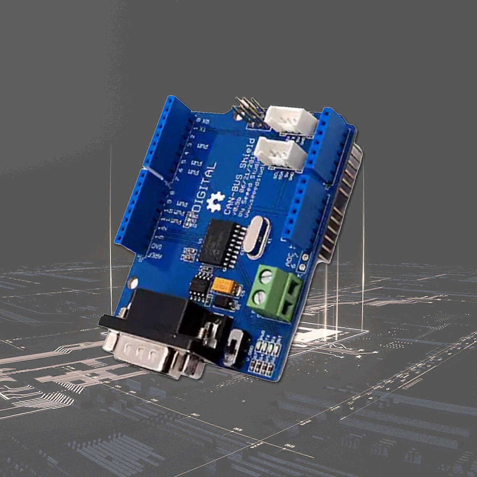
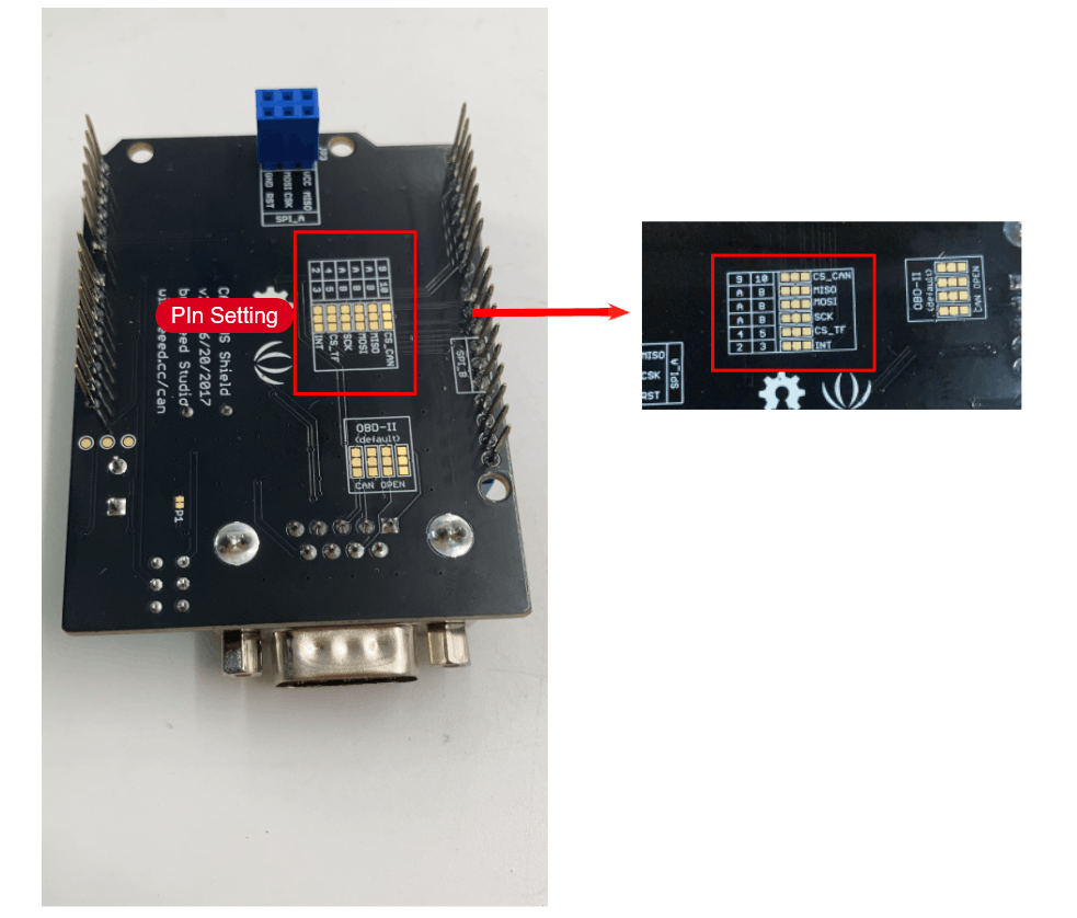
PCB Reverse Engineering for Side Road and Decoupling is a critical engineering practice when dealing with CAN Bus Communication PCBs used in excavators. These boards act as the backbone of machine electronics, linking sensors, actuators, engine controllers, and hydraulic modules through CAN and J1939 protocols. Because CAN networks operate in electrically noisy environments, proper side road routing and decoupling design are essential elements that must be carefully analyzed and preserved during reverse engineering.
Das Leiterplattenlayout wird digitalisiert, um die Layoutzeichnung zu rekonstruieren und präzise Gerber-Dateien sowie eine verifizierte Netzliste zu generieren. Besonderes Augenmerk liegt dabei auf CAN-Differenzialpaaren, Stichleitungslängen, Masseverbindung und lokaler Entkopplung in der Nähe der IC-Stromversorgungsanschlüsse. Diese Details sind entscheidend, wenn eine Kommunikationsplatine ohne Beeinträchtigung der Signalintegrität geklont, kopiert oder nachgebaut werden soll. Jede Abweichung in der Leiterbahngeometrie oder der Kondensatorplatzierung kann unter den rauen Betriebsbedingungen von Baggern zu Kommunikationsfehlern führen. Nach Abschluss der Dokumentation kann die Fertigung der unbestückten Leiterplatte beginnen. Die Leiterplatte wird gemäß der wiederhergestellten Gerber-Datei neu gefertigt, um eine gleichbleibende Kupferdicke und dielektrische Eigenschaften zu gewährleisten. Die Bauteilbeschaffung erfolgt anhand der wiederhergestellten Stückliste, die CAN-Transceiver, Schutzbauelemente, Oszillatoren und passive Entkopplungskomponenten umfasst. Sollten die Originalteile veraltet sein, können die Ingenieure Teile der Schaltung mit äquivalenten Komponenten überarbeiten oder neu gestalten und dabei die ursprüngliche Entkopplungsstrategie beibehalten.
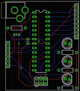
The reverse engineering workflow begins with a detailed inspection of the physical PCB to recover its electrical structure and signal topology. Engineers document board dimensions, layer count, impedance-controlled traces, and the placement of termination resistors and decoupling capacitors. From this analysis, the original schematic diagram is gradually restored, allowing engineers to understand how side road routing minimizes reflections and how decoupling networks stabilize power rails for transceivers and microcontrollers.
Le schéma du circuit imprimé est numérisé afin de recréer le plan d’implantation et de générer des fichiers Gerber précis ainsi qu’une netlist vérifiée. Une attention particulière est portée aux paires différentielles CAN, aux longueurs des stubs, à la continuité de la référence de masse et au découplage local à proximité des broches d’alimentation des circuits intégrés. Ces détails sont cruciaux pour cloner, copier ou répliquer une carte de communication sans altérer l’intégrité du signal. Toute variation dans la géométrie des pistes ou le placement des condensateurs peut entraîner des erreurs de communication dans les conditions d’utilisation difficiles d’une excavatrice. Une fois la documentation finalisée, la production de la carte nue peut commencer. Le circuit imprimé est refabriqué conformément au fichier Gerber restauré, garantissant ainsi une épaisseur de cuivre et des propriétés diélectriques constantes. L’approvisionnement en composants suit la nomenclature récupérée, qui comprend les émetteurs-récepteurs CAN, les dispositifs de protection, les oscillateurs et les composants de découplage passifs. Si les composants d’origine sont obsolètes, les ingénieurs peuvent remettre à neuf ou reconcevoir des sections du circuit en utilisant des composants équivalents tout en conservant la stratégie de découplage initiale.
Next, the PCB layout is digitized to recreate the layout drawing and generate accurate Gerber files and a verified netlist. Special attention is paid to CAN differential pairs, stub lengths, ground reference continuity, and local decoupling near IC power pins. These details are crucial when the goal is to clone, copy, or replicate a communication board without degrading signal integrity. Any deviation in trace geometry or capacitor placement can cause communication errors in harsh excavator operating conditions.
El diseño de la PCB se digitaliza para recrear el plano de diseño y generar archivos Gerber precisos y una lista de conexiones verificada. Se presta especial atención a los pares diferenciales CAN, las longitudes de los cables auxiliares, la continuidad de la referencia de tierra y el desacoplamiento local cerca de los pines de alimentación del CI. Estos detalles son cruciales cuando el objetivo es clonar, copiar o replicar una placa de comunicación sin degradar la integridad de la señal. Cualquier desviación en la geometría de la pista o la colocación del condensador puede causar errores de comunicación en las duras condiciones de funcionamiento de la excavadora. Una vez completada la documentación, puede comenzar la producción de la placa base. La PCB se remanufactura según el archivo Gerber restaurado, lo que garantiza un espesor de cobre y propiedades dieléctricas consistentes. La adquisición de componentes sigue la lista de materiales recuperada, que incluye transceptores CAN, dispositivos de protección, osciladores y componentes de desacoplamiento pasivo. Si las piezas originales están obsoletas, los ingenieros pueden reacondicionar o rediseñar secciones del circuito utilizando componentes equivalentes, manteniendo la estrategia de desacoplamiento original.
PCB Reverse Engineering for Side Road and Decoupling is a critical point to discuss in the circuit board layout redesigning, since side road and decoupling will affect the performance of Printed circuit board;
PCB Reverse Engineering will normally encounter the situation of side road and decoupling. Side road means transfer the unwanted common mode Radio frequency energy, the main function of side road capacitor is generate a AC component and eliminate the unnecessary energy which has entered the sensible area, decoupling means elimination of radio frequency which get access to the distribution network when switch the component. The major task of decoupling capacitor is provide a partial DC power supply to component and decrease the transmission on the switch noise when Reverse Engineering PCB and guide the noise onto ground.
PCB Reverse Engineering for Side Road and Decoupling is a critical point to discuss in the circuit board layout redesigning, since side road and decoupling will affect the performance of Printed circuit board
Selection of capacitor is a critical item:
When choosing the sideroad and decoupling capacitor, the value of capacitor can be chosen according to the frequency and capacitance, self-resonance frequency of capacitance calculated by logic series and the time clock speed. the SMT components should be given priority especially for those footprint with relative lower lead inductance instead of through hole components. Furthermore, engineer will usually choose parallel decoupling capacitor to provide more working band and decrease the imbalance grounding.
When Reverse Engineering PCB parallel capacitor system, if the working frequency higher than self resonance frequency, big capacitor will express the inductive impedance features and rise according to the increasing frequency; but the small capacitor will decrease the inductive capacitance accompany with increasing frequency.
Il layout del PCB viene digitalizzato per ricreare il disegno del layout e generare file Gerber accurati e una netlist verificata. Particolare attenzione viene prestata alle coppie differenziali CAN, alle lunghezze degli stub, alla continuità del riferimento di massa e al disaccoppiamento locale in prossimità dei pin di alimentazione del circuito integrato. Questi dettagli sono cruciali quando l’obiettivo è clonare, copiare o replicare una scheda di comunicazione senza compromettere l’integrità del segnale. Qualsiasi deviazione nella geometria della traccia o nel posizionamento dei condensatori può causare errori di comunicazione in condizioni operative difficili dell’escavatore. Una volta completata la documentazione, può iniziare la produzione della scheda nuda. Il PCB viene rifabbricato in base al file Gerber ripristinato, garantendo spessore del rame e proprietà dielettriche costanti. L’approvvigionamento dei componenti segue la distinta base recuperata, che include transceiver CAN, dispositivi di protezione, oscillatori e componenti di disaccoppiamento passivi. Se i componenti originali sono obsoleti, gli ingegneri possono ricondizionare o riprogettare sezioni del circuito utilizzando componenti equivalenti, mantenendo al contempo la strategia di disaccoppiamento originale.
the supreme court has already proclaimed the business secret or intellectual property obtained from self-research or through copying circuit card don’t belong to the unfair competition action. Circuit Engineering Co.,Ltd has commited to Reverse Engineering technology research and service for over two decades. and have ever reverse engineering then clone or copy the electronic printed circuit board from different industries, as well as the pcb board manufacture and prototype building. and we have great advantage over the cycle control, research and development as well as the cost analysis.
Nowadays, electronic products are being updated in fast speed; and PCB reverse engineering from our company in the base of completely master the traditional PCB structure or its basic circuit, furthermore, is base upon the self research and development, include the software upgrade and product second phase development;
And we will dedicate to clone PCB with 100% exact the same functions as original sample given by customers.at the same time, we also decrease the PCB reverse engineering cycle refers to the pcb board with blind or buried vias, effectively save customer time and energy, low down its cost. and which is also one of the reasons for us to be favor by most of our clients.