

PCB Board Reverse Engineering Tools
In recent days, pcb board reverse engineering tools have made some new breakthrough, some of the analysis tools have been developped regarding to the high speed design issue and pcb board reverse engineering. Take the software from INNOVEDA as the signal integrity analysis tool as reference, HYPERLYNX from this company has been charactered as easy to use, and can provide a powerful signal integrity analysis functions when reverse engineering pcb board. It has a very outstanding features is the user friendly operational interface which make the engineers can make analysis according to the their assumed scinerios when reverse engineering pcb board, and make the experiment on the terminal topology issues, through which the best solutions can be found after the features and reliability can be satisfied swiftly. As for those engineers who need to reverse engineering pcb board with high complexity and system, XTK signal integrity verification tools set from the INNOVEDA and signal integrity planning environment EPLANNER can provide a advanced algorithm and other more mature validation functions which can be used on the super speed signal integrity analysis of pcb board reverse engineering, include the topology analysis, high speed scanning or consumption, and other high level algorithm for signal integrity analysis.
In the past, engineers must make a choise between the HYPERLYNE and XTK when reverse engineering pcb board. In recent days, INNOVEDA can make the connections of these two tools of critical signal integrity scanning into realization, this connections can make the integrate together, and they can be used simutaneously when reverse engineering pcb board and consequently shorten the pcb board reverse engineering cycle. Generally speaking, HYPERLYNX has been used as the signal analysis tools for high speed PCB board reverse engineering, however, XTK and eplanner will be used to proceed the topology analysis and restricted terms when reverse engineering pcb board.
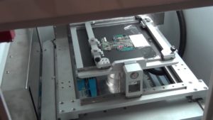
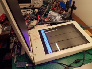
pcb x-ray scanning machine which used to view the inner layer circuitry pattern when reverse engineering multilayer pcb
the supreme court has already proclaimed the business secret or intellectual property obtained from self-research or through reverse engineering PCB don’t belong to the unfair competition action. Circuit Engineering Co.,Ltd has commited to Reverse Engineering technology research and service for over two decades. and have ever reverse engineering then clone or copy the electronic printed circuit board from different industries, as well as the pcb board manufacture and prototype building. and we have great advantage over the PCB reverse engineering cycle control, research and development as well as the cost analysis.
Nowadays, electronic products are being updated in fast speed; and PCB reverse engineering from our company in the base of completely master the traditional PCB structure or its basic circuit, furthermore, is base upon the self research and development, include the software upgrade and product second phase development; and we will dedicate to clone PCB with 100% exact the same functions as original sample given by customers.at the same time, we also decrease the PCB reverse engineering cycle refers to the pcb board with blind or buried vias, effectively save customer time and energy, low down its cost. and which is also one of the reasons for us to be favor by most of our clients.
Tags: copy circuit board,copy circuit card,copy pcb,copy pcb assemble,copy pcb board,copy pcb card,copy pcb circuit board,copy pcba,copy printed circuit board,copy printed wiring board,copy pwb