

Multi-Layer Printed Circuit Board Stack-Up Rules
Multi-Layer Printed Circuit Board Stack-Up Rules needs to be followed in order to carry out a proper and stable electrical performance of Multilayer PCB board design cloning;
By stacking two layers, the top layer (ie, layer 1) is used as a signal layer.
The four-layer stack uses the top and bottom layers (or the 1st and 4th layers) as the signal layer.
In this configuration, the 2nd and 3rd layers are used as planes. The prepreg layer bonds two or more double-sided panels together and acts as a dielectric between the layers.
The six-layer PCB adds two copper layers, and the second and fifth layers serve as planes. Layers 1, 3, 4, and 6 carry signals.
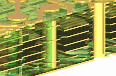
Proceed to the six-layer structure, the inner layer two, three (when it is a double-sided circuit board design drawing reversing) and the fourth five (when it is a double-sided board) as the core layer, and the prepreg (PP) is sandwiched between the core boards.
Since the prepreg material has not been fully cured, the material is softer than the core material. The PCB manufacturing process applies heat and pressure to the entire stack and melts the prepreg and core so that the layers can be bonded together.
Multilayer PCB boards add more copper and dielectric layers to the stack. In an eight-layer PCB, the seven inner rows of the dielectric glue the four planar layers and the four signal layers together.
Ten to twelve-layer boards increase the number of dielectric layers, retain four planar layers, and increase the number of signal layers.