"Everything we build starts with design engineering. CECL manufactured boards for one of our products. It went perfectly – a real success.It is really an high quality service they have provided to us!"
By Nile Smith from Sinotech Inc.
“We had several very old device with obsolete boards need to be replaced –through CECL professional service.We got what we needed, and we’ve been using the results of the work without any problem till now.”
By Richard Anderson from TWP system Inc.
"Guys from CECL manufacture PCBs we use in one of our products, a clinometer and we’ve never had a problem with anything. The boards come in, they work. And, their team is very responsive."
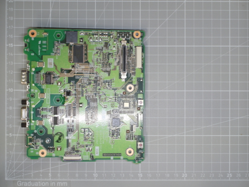
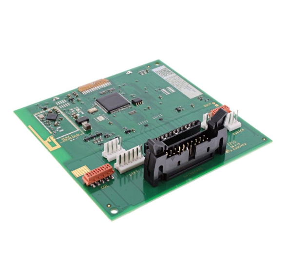
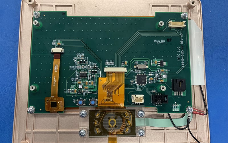
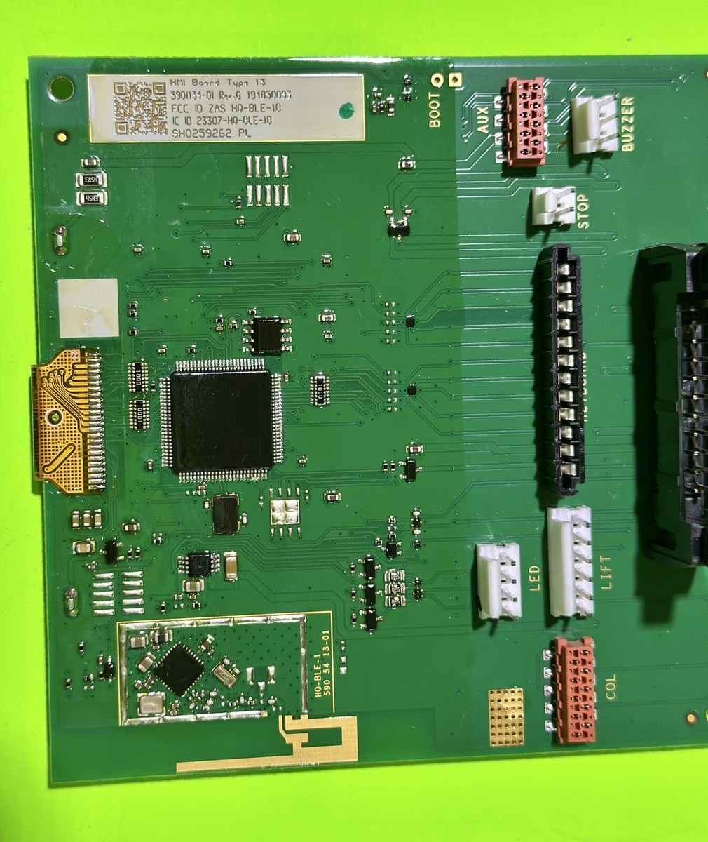
In the world of heavy machinery, the backhoe loader represents a critical piece of equipment where operator control and monitoring directly impact productivity and safety. The Display and Human-Machine Interface boards that connect to LCD/TFT panels are essential components that often face obsolescence challenges. When original manufacturing data is lost or suppliers discontinue these specialized boards, reverse engineering becomes the most viable path forward. This process enables teams to recover the intellectual property embedded in existing hardware, starting with the physical PCB and working backward to recreate the complete design package including Gerber files, schematic diagrams, and layout drawings.
Wenn die ursprünglichen Fertigungsdaten verloren gehen oder die Hersteller die Produktion dieser speziellen HMI-Leiterplatten einstellen, ist Reverse Engineering der erfolgversprechendste Weg. Dieses Verfahren ermöglicht es Teams, das in der vorhandenen Hardware enthaltene geistige Eigentum wiederherzustellen. Ausgehend von der physischen Leiterplatte wird das gesamte Designpaket inklusive Gerber-Dateien, Schaltplänen und Layoutzeichnungen rekonstruiert. Die Reproduktion einer Hochgeschwindigkeits-Display-Leiterplatte beginnt mit der sorgfältigen Dokumentation der bestehenden Baugruppe. Ingenieure müssen zunächst eine präzise Stückliste erstellen, indem sie jede Komponente auf der Platine identifizieren – vom Grafikcontroller bis hin zu den passiven Filternetzwerken, die saubere Videosignale zum LCD-Panel gewährleisten. Mithilfe spezieller Scangeräte und Software erfassen Techniker jede Lage der Multilayer-Platine und schaffen so die Grundlage für die exakte Nachfertigung der Leiterbahnen und Durchkontaktierungen. Dieses optische Scanverfahren erhält die kritischen Hochgeschwindigkeitssignalwege, die die Impedanzkontrolle für die Differenzialpaare gewährleisten, welche die Pixeldaten zum TFT-Display übertragen. Ziel ist es nicht nur, das visuelle Erscheinungsbild zu kopieren, sondern die präzisen elektrischen Eigenschaften zu reproduzieren, die einen zuverlässigen Betrieb in der vibrationsreichen Umgebung einer Baggerkabine sicherstellen.
Most of the High Speed PCB reverse engineering will include some functionality sub-system or areas, each one of the functional sub-system is constituted by a series of parts and their supported circuit. For example, a typical mainboard PCB reverse engineering can be divided into: processor, clock logic, memorizer, data-bus controller, data-bus terminal, PCT data-bus, peripheral terminal and video/audio block, etc. from one side, PCB reverse engineering need to make sure all of the components place close to each other, it can help to shorten the circuit when reverse engineering PCB, low down the cross-talk, reflection even electro-magnetic radiation and keep the signal integrity; from other side, the spectrum generated by Radio frequency from different logic part is various too, especially in the high speed PCB reverse engineering system, the higher the signal frequency, the radio frequency energy bandwidth generated from the digital signal jump operation is wider for PCB reverse engineering, so in order to prevent the mutual interference among different components which has various bandwidth, High Speed PCB reverse engineering rules must be draw and carefully preserved.
Lorsque les données de fabrication originales sont perdues ou que les fournisseurs cessent la production de ces cartes de circuits imprimés IHM spécialisées, la rétro-ingénierie devient la solution la plus viable. Ce processus permet aux équipes de récupérer la propriété intellectuelle intégrée au matériel existant, en partant du circuit imprimé physique et en remontant la chaîne pour recréer l’ensemble du dossier de conception, y compris les fichiers Gerber, les schémas et les plans d’implantation. La reproduction d’une carte de circuit imprimé pour écran haute vitesse commence par une documentation méticuleuse de l’assemblage existant. Les ingénieurs doivent d’abord établir une nomenclature précise en identifiant chaque composant de la carte, du contrôleur graphique principal aux réseaux de filtrage passif qui garantissent la qualité des signaux vidéo vers la dalle LCD. À l’aide d’équipements et de logiciels de numérisation spécialisés, les techniciens peuvent capturer chaque couche de la carte multicouche, créant ainsi la base nécessaire à la reproduction exacte des pistes de cuivre et de l’emplacement des vias. Ce processus de numérisation optique préserve les chemins de signaux haute vitesse critiques qui assurent le contrôle d’impédance des paires différentielles transportant les données des pixels vers l’écran TFT. L’objectif n’est pas seulement de copier l’apparence visuelle, mais aussi de reproduire les caractéristiques électriques précises qui garantissent un fonctionnement fiable dans l’environnement vibrant d’une cabine de pelle rétro.
The journey to reproduce a high-speed display board begins with meticulous documentation of the existing assembly. Engineers must first generate an accurate BOM list by identifying every component on the board, from the main graphics controller to the passive filtering networks that ensure clean video signals to the LCD panel. Using specialized scanning equipment and software, technicians can capture each layer of the multilayer board, creating the foundation needed to remanufacture the exact copper traces and via placements. This optical scanning process preserves the critical high-speed signal paths that maintain impedance control for the differential pairs carrying pixel data to the TFT display. The goal is not merely to copy the visual appearance but to replicate the precise electrical characteristics that ensure reliable operation in the vibration-rich environment of a backhoe cab.
Quando i dati di produzione originali vengono persi o i fornitori interrompono la produzione di queste schede HMI specializzate, il reverse engineering diventa la strada più praticabile. Questo processo consente ai team di recuperare la proprietà intellettuale incorporata nell’hardware esistente, partendo dal PCB fisico e lavorando a ritroso per ricreare il pacchetto di progettazione completo, inclusi file Gerber, diagrammi schematici e disegni di layout. Il percorso per riprodurre una scheda PCB per display ad alta velocità inizia con una documentazione meticolosa dell’assemblaggio esistente. Gli ingegneri devono innanzitutto generare un elenco BOM accurato identificando ogni componente sulla scheda, dal controller grafico principale alle reti di filtraggio passivo che garantiscono segnali video puliti al pannello LCD. Utilizzando apparecchiature e software di scansione specializzati, i tecnici possono acquisire ogni strato della scheda multistrato, creando le basi necessarie per ricostruire le tracce di rame e i posizionamenti dei via esatti. Questo processo di scansione ottica preserva i percorsi critici del segnale ad alta velocità che mantengono il controllo dell’impedenza per le coppie differenziali che trasportano i dati dei pixel al display TFT. L’obiettivo non è semplicemente copiare l’aspetto visivo, ma replicare le precise caratteristiche elettriche che garantiscono un funzionamento affidabile nell’ambiente ricco di vibrazioni della cabina di un escavatore.
Circuit Engineering Co.,Ltd. is dedicated to delivering the highest quality Printed Circuit Board Reverse Engineering, PCB Clone, PWB Copy, Printed Wiring Board Duplication, PCB Card Replication services with an approach that is tailored to meet the needs of medium sized OEMs. We specialize in turnkey manufacturing of high mix, high complexity products for military, avionics, industrial, medical, and energy management markets. Circuit Engineering Co.,Ltd.’s history of building strong partnerships and developing flexible solutions differentiates us from the rest of the EMS industry.
Orijinal üretim verileri kaybolduğunda veya tedarikçiler bu özel HMI devre kartlarını üretmeyi bıraktığında, tersine mühendislik en uygun çözüm yolu haline gelir. Bu süreç, ekiplerin mevcut donanımda gömülü fikri mülkiyeti kurtarmasını sağlar; fiziksel PCB’den başlayarak geriye doğru çalışarak Gerber dosyaları, şematik diyagramlar ve yerleşim çizimleri de dahil olmak üzere eksiksiz tasarım paketini yeniden oluşturur. Yüksek hızlı bir ekran PCB kartının yeniden üretilmesi yolculuğu, mevcut montajın titiz bir şekilde belgelenmesiyle başlar. Mühendisler öncelikle, ana grafik denetleyicisinden LCD panele temiz video sinyalleri sağlayan pasif filtreleme ağlarına kadar kart üzerindeki her bileşeni tanımlayarak doğru bir malzeme listesi (BOM) oluşturmalıdır. Özel tarama ekipmanı ve yazılımı kullanarak, teknisyenler çok katmanlı kartın her katmanını yakalayabilir ve tam bakır izlerini ve geçiş noktalarını yeniden üretmek için gereken temeli oluşturabilirler. Bu optik tarama işlemi, piksel verilerini TFT ekrana taşıyan diferansiyel çiftler için empedans kontrolünü sağlayan kritik yüksek hızlı sinyal yollarını korur. Amaç sadece görsel görünümü kopyalamak değil, aynı zamanda bir kazıcı kabininin titreşim açısından zengin ortamında güvenilir çalışmayı sağlayan hassas elektriksel özellikleri de kopyalamaktır.
Our passionate people and efficient processes support aggressive new product introduction timelines, and a smooth transition of those products into production. Employees are empowered to deliver superior program management, supply chain management, exceptional workmanship quality, efficient test strategies, and final assembly and packaging solutions that ensure the successful PCB reverse engineering, PCB Board Clone, PCB Assemble Copy, Printed Circuit Board Replicate, Printed Wiring Board Duplicate engineering and manufacturing and on-time delivery of your products.
Once the physical layer data is captured, the more complex task of extracting logical connectivity begins. Advanced netlist extraction tools analyze the scanned layer images to determine how each component pin connects to others, effectively recovering the hidden netlist that defines the board’s functionality. This step is particularly challenging for display interfaces where high-speed signals must maintain specific routing constraints. Engineers may use flying probe testers to verify continuity on critical paths, ensuring that the recreated netlist accurately reflects the original design intent. Simultaneously, the team works to restore the schematic diagram by tracing connections from the main processor through the memory devices, level shifters, and finally to the LCD connector. This intellectual property recovery transforms a physical board into editable design files that can be modified for future improvements.
With verified connectivity established, the focus shifts to generating the complete manufacturing documentation package. This includes finalizing the layout drawings with precise component placements that account for mechanical constraints within the backhoe’s operator station. The schematic diagram is meticulously redrawn in modern CAD tools, documenting not just connections but also the design intent behind filtering networks and power distribution. Engineers also refurbish the BOM list to address component obsolescence, often substituting long-discontinued display drivers with modern equivalents that maintain form, fit, and function. The culmination of this effort is a complete set of Gerber files that can be sent directly to fabrication houses, enabling the client to remanufacture boards on demand without dependency on original suppliers.
जब ओरिजिनल मैन्युफैक्चरिंग डेटा खो जाता है या सप्लायर इन खास HMI सर्किट बोर्ड को बंद कर देते हैं, तो रिवर्स इंजीनियरिंग सबसे सही रास्ता बन जाता है। यह प्रोसेस टीमों को मौजूदा हार्डवेयर में एम्बेडेड इंटेलेक्चुअल प्रॉपर्टी को रिकवर करने में मदद करता है, जो फिजिकल PCB से शुरू होता है और Gerber फाइल्स, स्कीमैटिक डायग्राम और लेआउट ड्रॉइंग सहित पूरे डिज़ाइन पैकेज को फिर से बनाने के लिए पीछे की ओर काम करता है। हाई-स्पीड डिस्प्ले PCB बोर्ड को फिर से बनाने का सफर मौजूदा असेंबली के बारीकी से डॉक्यूमेंटेशन से शुरू होता है। इंजीनियरों को सबसे पहले बोर्ड पर हर कंपोनेंट की पहचान करके एक सटीक BOM लिस्ट बनानी होगी, मेन ग्राफिक्स कंट्रोलर से लेकर पैसिव फिल्टरिंग नेटवर्क तक जो LCD पैनल को साफ वीडियो सिग्नल सुनिश्चित करते हैं। खास स्कैनिंग इक्विपमेंट और सॉफ्टवेयर का इस्तेमाल करके, टेक्नीशियन मल्टीलेयर बोर्ड की हर लेयर को कैप्चर कर सकते हैं, जिससे सटीक कॉपर ट्रेस और वाया प्लेसमेंट को फिर से बनाने के लिए ज़रूरी फाउंडेशन तैयार होता है। यह ऑप्टिकल स्कैनिंग प्रोसेस उन ज़रूरी हाई-स्पीड सिग्नल पाथ को सुरक्षित रखता है जो TFT डिस्प्ले पर पिक्सल डेटा ले जाने वाले डिफरेंशियल पेयर के लिए इम्पीडेंस कंट्रोल बनाए रखते हैं। इसका मकसद सिर्फ दिखने वाले लुक को कॉपी करना नहीं है, बल्कि उन सटीक इलेक्ट्रिकल कैरेक्टरिस्टिक्स को कॉपी करना है जो बैकहो कैब के वाइब्रेशन-रिच माहौल में भरोसेमंद ऑपरेशन सुनिश्चित करते हैं।
The final phase ensures that the redeveloped board performs identically to the original in the demanding backhoe environment. Test fixtures validate that the replicated display interface maintains proper timing and voltage levels to the LCD panel, while environmental chambers confirm that the recreated design withstands temperature extremes and mechanical shock. For equipment owners, successful reverse engineering of these HMI boards means extended machine life and reduced downtime. Having the complete design package—Gerber files, schematic diagrams, layout drawings, BOM list, and netlist—restores full control over the supply chain. Whether the need is to clone an existing board for inventory, duplicate a design for a fleet upgrade, or simply recover documentation for future maintenance, professional reverse engineering delivers a permanent solution to component obsolescence in critical heavy equipment applications.