

High Density PCB Board Layout
High Density PCB Board Layout
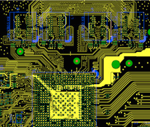
Refers to the high density PCB Board Layout, it is not applicable to use the through hole technique, since it waste tremendous layout route resource; in order to solve this conflict, the emergency of blind and buried VIAs technique can not only accomplish the effect of through hole, it will also save great amount of layout route space for a more convenient, more smooth Layout result; the process of High density PCB Board layout is a complicate but simple one, which will require the engineer to have more experience in the work.
High Density PCB Board Layout
The yielding rate of automatic layout PCB Board depends on the a rational and proper layout placement, the rules can be pre-set, include the times of wiring curve, quantity of through hole, number of stepping, etc. normally explosive layout will be taken and connect those short wires together swiftly, then proceed with maze layout; optimize the layout route as a whole then re-layout the structure to improve the comprehensive effect;