

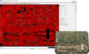
Featured Impedance in PCB Reverse Engineering
Featured Impedance in PCB Reverse Engineering has described how the process variation affect the actual change on featured impedance, as well as how to use the precise field solver tools to foresee this kind of phenomenon.
Even without the process variation, other factors can trigger the great change of the featured impedance. So in the process of PCB Reverse Engineering, automatic design tools will occasionally not able to detect these kinds of issues sometimes not very obvious but extremely important.
Featured Impedance in PCB Reverse Engineering
However, as long as some necessary measures have been taken in the preliminary stage of Printed Circuit Board Reverse Engineering can effectively avoid these issues which can viewed as defensive tactics;
First of all we can introduce this measure call layer count issue, a excellent layer structure is the best defensive measures for most of the signal integrity issue and EMC issue, meanwhile it is easily to be misunderstood. And there are several other factors is playing the effect, solve one with the proper measure will properly deteriorate the others.
As a result of that, most of the systematic designer will suggest there must be at least one consistent plane in the PCB to control featured impedance and signal quality, as long as the cost is affordable, it could be a very good advice.
Electro-magnetic consultancy will frequently suggest to place the ground fill on the outer layer or using ground layer to control the electro-magnetic radiation and its sensitivity to the electro-magnetic interference, for which is an effective solution;