


AI Server High Speed Printed Circuit Board Reverse Engineering for HDI System Reconstruction
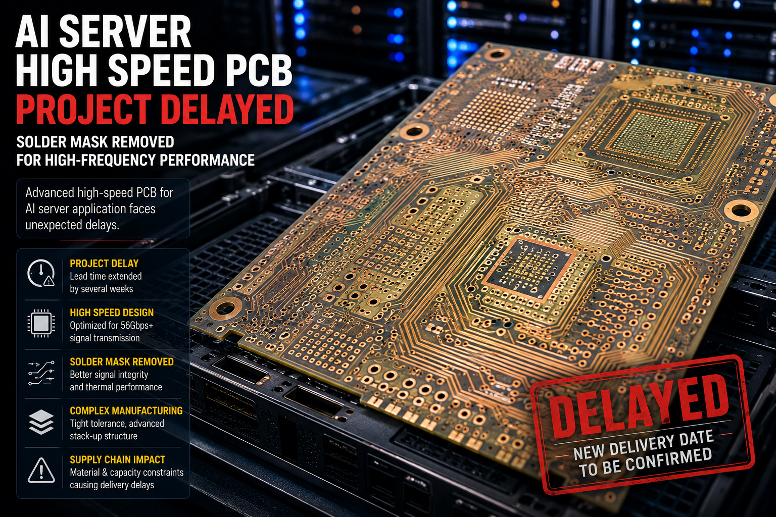
The explosive growth of artificial intelligence has triggered an unprecedented demand for high-density interconnect (HDI) printed circuit boards. These complex platforms anchor the high-speed signaling and massive processing power required by modern AI clusters. However, legacy hardware maintenance, competitive analysis, and supply chain security often require teams to deconstruct this advanced hardware. Implementing AI compute High Speed Printed Circuit Board Reverse Engineering allows engineering firms to dissect these dense layouts, offering a structured methodology to analyze, protect, and iterate on cutting-edge hardware design.
Partendo da questa netlist, gli ingegneri lavorano a ritroso per replicare lo schema elettrico originale del PCB HDI per calcolo AI, creando una gerarchia leggibile che mostra come i processori AI interagiscono con i sottosistemi di memoria.
Parallelamente, i componenti vengono dissaldati e identificati per compilare una BOM list (Bill of Materials) accurata, consentendo ai team di duplicare la strategia di approvvigionamento dei componenti del PCB HDI per calcolo AI oppure di rigenerare hardware obsoleto utilizzando equivalenti moderni.
Deconstructing the Hardware: From Physical Board to Digital Assets
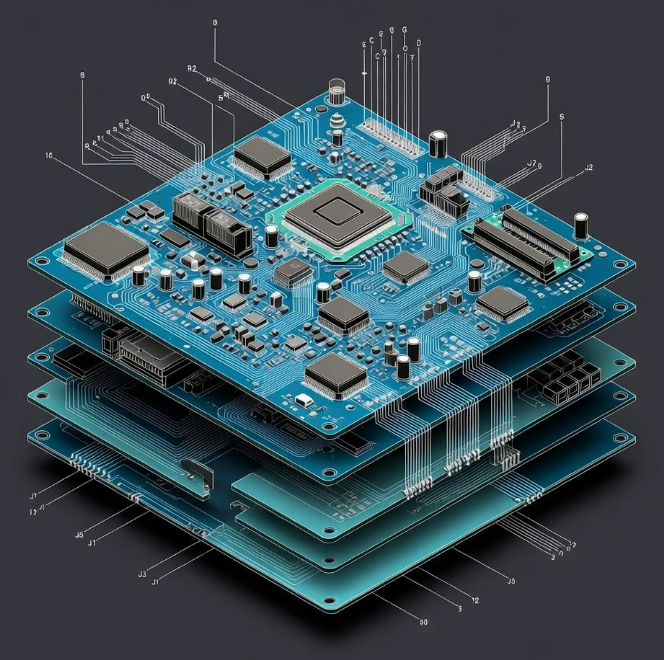
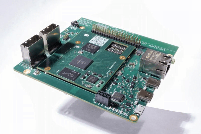
To successfully reverse engineering a multi-layered AI accelerator card, engineers must bridge the gap between physical silicon placement and digital blueprints. The process begins with meticulous non-destructive imaging and automated layer-by-layer delamination. Through this process, hardware teams aim to recover the exact physical topology of the board. The primary objective is to restore missing documentation by extracting the raw geometric data, which is then used to recreate the precise layout drawing. By tracing microvias and buried traces under high-density BGA packages, specialists can systematically reproduce the complex connectivity maps essential for high-speed signal integrity.
À partir de cette netlist, les ingénieurs réalisent une reconstruction inverse du schéma électrique original de la carte HDI de calcul IA, établissant une hiérarchie lisible illustrant l’interaction entre les processeurs IA et les sous-systèmes mémoire.
Parallèlement, les composants sont dessoudés puis identifiés afin d’établir une liste BOM (Bill of Materials) précise, permettant aux équipes de reproduire la stratégie d’approvisionnement des composants de la carte HDI de calcul IA ou de remettre à niveau du matériel vieillissant avec des équivalents modernes.
Printed Circuit Board dimension has the trend to shrink their sizes while their functionality has been increased too, at the same time, the clock rate and component rising time become faster. High speed PCB design has become a important part of it. In order to solve these problems generated from the daily populated high speed Printed Circuit Board design, the key is using the signal analysis as basis, combine with the swift inspection in the design end stage to fulfill the comprehesive design method.
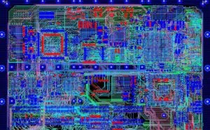
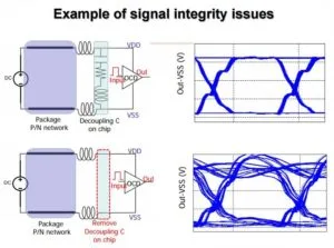
Most of the design engineers are all familiar with the high speed Printed Circuit Board design as well as the reliability issue involved in it. However, when they try to solve the critical circuit network issue is still depends on their experience. And few of them will combine the high speed analysis into the design which can’t be ignored anymore, GHZ rate clock, high speed system databus, decreasing physical dimension which bring more and more difficult, especially the most commonly use Printed Circuit Board will face the signal integrity issue.
Reconstructing System Intelligence: Schematics, Netlists, and BOMs
Once the physical geometry is digitized, the focus shifts to logical reconstruction. Software suites process the vectorized layout drawing to generate a comprehensive netlist, mapping every electrical connection across the high-speed channels. This data is invaluable to clone the exact functional routing or to copy specific power delivery networks. From this netlist, engineers work backward to replicate the original schematic diagram, establishing a readable hierarchy of how the AI processors interact with memory subsystems. Concurrently, components are desoldered and identified to compile an accurate bom list (Bill of Materials), allowing teams to duplicate the component sourcing strategy or refurbish aging hardware with modern equivalents.
A partir de esta netlist, los ingenieros trabajan en sentido inverso para replicar el diagrama esquemático original del PCB HDI para computación de IA, estableciendo una jerarquía legible que muestra cómo los procesadores de IA interactúan con los subsistemas de memoria.
Simultáneamente, los componentes se desueldan e identifican para elaborar una lista BOM (Bill of Materials) precisa, permitiendo a los equipos duplicar la estrategia de abastecimiento de componentes del PCB HDI para computación de IA o reacondicionar hardware envejecido utilizando equivalentes modernos.
Maximizing the Deliverables: Manufacturing and Redevelopment
With the schematic diagram, bom list, and netlist fully validated, the project transitions from analysis to actionable manufacturing assets. These files are converted into an industry-standard Gerber file, the universal language for PCB fabrication houses. Armed with a production-ready Gerber file, organizations can choose to remanufacture the board to maintain legacy systems, or replicate the architecture for localized testing. Beyond simple duplication, the ultimate value of this process lies in redevelopment. Engineers can leverage the extracted data to redesign specific subsystems—such as optimizing thermal dissipation or upgrading power rails—ensuring the hardware evolves alongside rapidly advancing AI workloads.
На основе этой netlist инженеры выполняют обратное восстановление исходной принципиальной схемы HDI-платы для вычислений ИИ, формируя понятную иерархию взаимодействия процессоров ИИ с подсистемами памяти.
Одновременно выполняется демонтаж и идентификация компонентов для составления точного BOM-списка (Bill of Materials), что позволяет командам воспроизводить стратегию выбора компонентов оригинальной HDI-платы для вычислений ИИ либо модернизировать устаревшее оборудование с использованием современных аналогов.
The Strategic Value of Advanced Board Decoupling
Ultimately, Mastering AI compute High Speed Printed Circuit Board Reverse Engineering is about more than creating a carbon copy of existing technology. It provides a foundational blueprint that empowers organizations to safeguard their supply chains, verify intellectual property, and bridge the gap between generations of hardware. Whether the goal is to clone a critical component for redundancy, refurbish deployed infrastructure, or completely redesign a high-speed interface for next-generation chips, extracting the Gerber file and system logic transforms hidden hardware into an open platform for innovation.
Com base nesta netlist, os engenheiros trabalham de forma reversa para reproduzir o diagrama esquemático original da placa HDI de computação para IA, estabelecendo uma hierarquia legível de como os processadores de IA interagem com os subsistemas de memória.
Em paralelo, os componentes são dessoldados e identificados para compilar uma lista BOM (Bill of Materials) precisa, permitindo às equipes duplicar a estratégia de fornecimento de componentes da placa HDI de computação para IA ou renovar hardware antigo utilizando equivalentes modernos.