

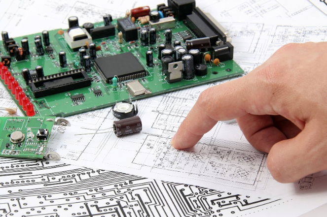
Analog Printed Circuit Board Layout Reverse Engineering
In Analog Printed Circuit Board Layout Reverse Engineering, bypass capacitors are usually used to bypass high-frequency signals on the power supply. If bypass capacitors are not added, these high-frequency signals may enter sensitive analog chips through the power supply pins.
Generally speaking, the frequency of these high-frequency signals exceeds the ability of analog devices to suppress high-frequency signals. If bypass capacitors are not used in the Analog Printed Circuit Board design drawing cloning, noise may be introduced in the signal path, and more serious cases may even cause vibration.
Below Figure In analog and digital PCB design, bypass or decoupling capacitors (0.1µF) should be placed as close as possible to the device. The power supply decoupling capacitor (10µF) should be placed at the power line entrance of the circuit board. In all cases, the pins of these capacitors should be short.
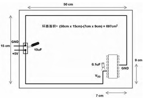
Below Figure On this circuit board, different routes are used to route the power and ground wires. Due to this improper cooperation, the electronic components and circuits on the circuit board are more likely to be subject to electromagnetic interference.
