

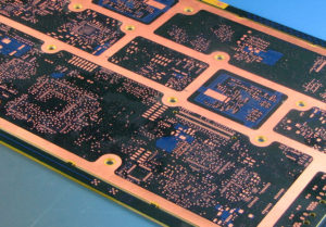
High Frequency PCB Board Reverse Engineering
In High Frequency PCB Board Reverse Engineering, the inductance of back route will be the main part of track resistance, as a result of that, when reverse engineering the high frequency PCB board, if the reverse engineeringer intend to minimize the grounding impedance should choose the multipoint grounding. The most important thing of Multipoint grounding is ensure the grounding track as short as possible since the longer the grounding track, the higher the impedance value and cause the grounding potential difference.
High Frequency PCB Board Reverse Engineering
Separate the analog and digital circuit, there are high speed logic circuit and liner circuit on the PCB board, engineer should do the best to separate them and ensure there is no mixture among them, and connect with the power supply terminal. Low frequency circuit’s grounding track should use single point parallel grounding, and make the grounding track as wide and short as possible, Big grid shape of copper track being applied around high frequency component. And increase the grounding area of the liner track.
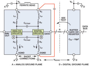
Separate the analog and digital circuit
4> Grounding track become the round cycle look: when reverse engineering the grounding track system constituted by digital circuit of PCB board. The noise resistance capability can effectively increased once reverse engineering the grounding track into block circuit. Since there are tremendous integrated circuit components on the PCB board especially for those with more power consumption will generate great potential difference on the grounding track due to the limitation of its width and space and cause the deterioration of noise resistance and form loop back on the grounding track.
Tags: pcb assemble reverse engineering,pcb board reverse engineering,pcb card reverse engineering,pcb reverse engineering,pcba reverse engineering,Printed Circuit Board Reverse Engineering,printed wiring board reverse engineering,pwb reverse engineering,pwba reverse engineering