reverse engineering pcb board layout
-
High Density Interconnect Printed Circuit Card Reverse Engineering
First of all it is High Density Interconnect Printed Circuit Card Reverse Engineering: The quantity increasing of Semiconductor’s complexity and logic gate will require the integrated circuit to embed with more and more pin-outs and finer patch among...
-
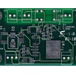
PCB Reverse Engineering Initial Measurement
PCB Reverse Engineering initial measurement is an critical process prior to disassembly, all dimensions and electronic data should be recorded, such as orientation of each components on the schematic diagram extracted from PCB board, like inductor an...
-
Printed Wiring Board Cloning Production
In the electronic production and design industry there is a popular and widely accepted reason: from the Printed wiring board Cloning to the production stage, repetitive work’s cost can be increased by index, and once these products flow into the si...
-
Electronic PCB Card Cloning Signal Integrity
Electronic PCB Card Cloning Signal Integrity is a very important topic to be discussed in the process of PCB reverse engineering, we have discussion with tremendous engineers and they are always mumbling and keep on telling you how much dangers the ...