

Symmetric Stripline Transmission Lines in the PCB Reverse Engineering
Symmetric Stripline Transmission Lines in the PCB Reverse Engineering
A method of PCB Reverse Engineering preferred from many viewpoints is a multilayer PCB. This arrangement embeds the signal trace between a power and a ground plane, as shown in the cross-sectional view of below Figure. The low impedance ac-ground planes and the embedded signal trace form a symmetric stripline transmission line.
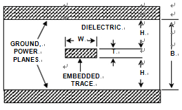
A Symmetric Stripline Transmission Line With Defined Impedance
As can be noted from the figure, the return current path for a high frequency signal trace is located directly above and below the signal trace on the ground/power planes. The high frequency signal is thus contained entirely inside the PCB, minimizing emissions, and providing natural shielding against incoming spurious signals. The characteristic impedance of this arrangement is again dependent upon geometry and the εr of the PCB dielectric. An expression for ZO of the stripline transmission line is:
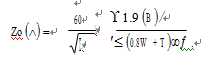
Here, all dimensions are again in mils, and B is the spacing between the two planes. In this symmetric geometry, note that B is also equal to 2H + T. Reference 17 indicates that the accuracy of this Reference 16 equation is typically on the order of 6%.
Another handy guideline for the symmetric stripline in anr = 4.0 case is to make B a multiple of W, in the range of 2 to 2.2. This will result in an stripline impedance of about 50. Of course this rule is based on a further approximation, by neglecting T. Nevertheless, it is still useful for ballpark estimates.
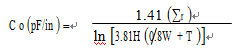
The symmetric stripline also has a characteristic capacitance, which can be calculated in terms of pF/in:
The propagation delay of the symmetric stripline is shown in below Equation.
![]()
or, in terms of ps:
For a PCB dielectric constant of 4.0, it can be noted that the symmetric stripline’s delay
constant is almost exactly 2 ns/ft, or 170 ps/in.