

Shock Wave Resistance Circuit in PCB Board Reverse Engineering
Shock Wave Resistance Circuit in PCB Board Reverse Engineering
Filtering the shock wave circuit is shown in below Figure.
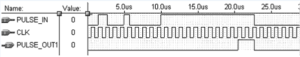
When a positive transition occurs on the PULSE_IN terminal, the upper edge causes the output of the flip-flop D1 to generate a high level signal, and the start counter starts counting.
When the counter is full, the counter output generates a positive transition. The rising edge causes the output of the flip-flop D3 to generate a high-level signal by Shock Wave Resistance Circuit in PCB Board Reverse Engineering, and the two signals are combined to obtain the output signal PULSE_OUT1.
Shock Wave Resistance Circuit in PCB Board Reverse Engineering
When the falling edge of PULSE_IN comes, the counter and three flip-flops are cleared at the same time, waiting for the next signal to arrive. As can be seen from FIG. 2, when the pulse width of PULSE_IN is less than the set timing width, the interference signal PULSE_OUT1 is considered to be low;
When the pulse width of PULSE_IN is greater than the set timing width and is still high, the signal is considered to be valid, PULSE_OUT1 is high and The falling edge of PULSE_IN goes low, waiting for the next signal to arrive.