"Everything we build starts with design engineering. CECL manufactured boards for one of our products. It went perfectly – a real success.It is really an high quality service they have provided to us!"
By Nile Smith from Sinotech Inc.
“We had several very old device with obsolete boards need to be replaced –through CECL professional service.We got what we needed, and we’ve been using the results of the work without any problem till now.”
By Richard Anderson from TWP system Inc.
"Guys from CECL manufacture PCBs we use in one of our products, a clinometer and we’ve never had a problem with anything. The boards come in, they work. And, their team is very responsive."
Reverse Engineering Printed Wiring Board for Signal Integrity
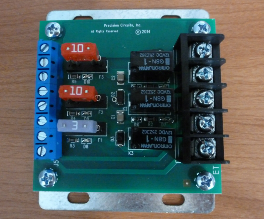
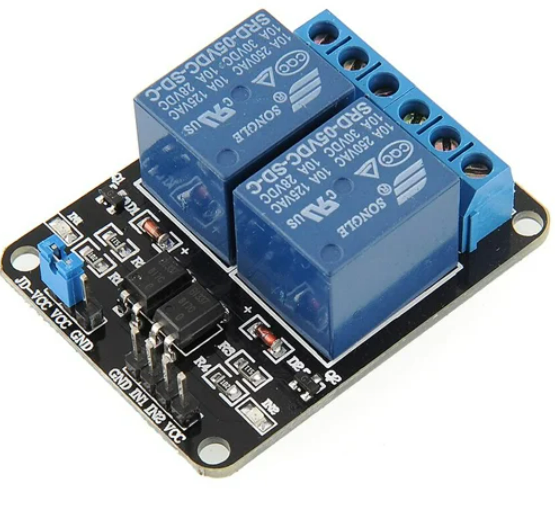
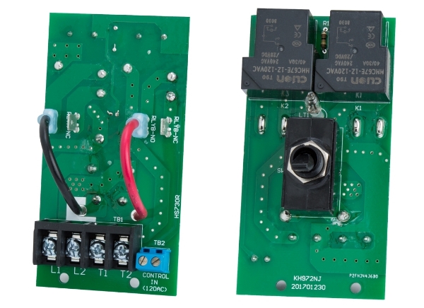
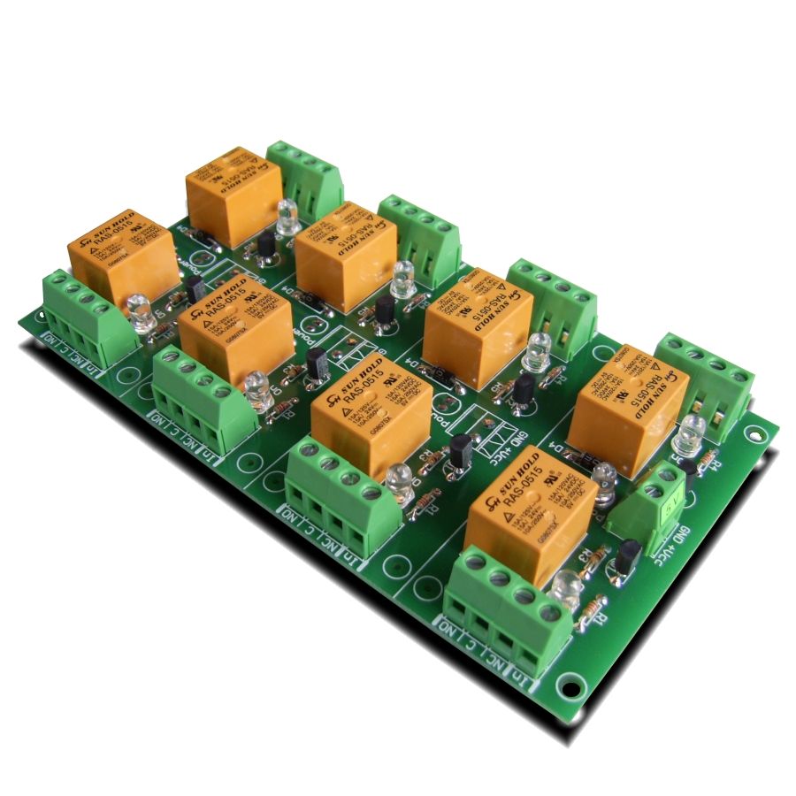
Reverse engineering printed wiring board assemblies for signal integrity is a specialized discipline, particularly when applied to power distribution and relay control PCBs used for auxiliary functions and lighting control in wheel loaders. These circuit boards manage current routing, relay triggering, fuse protection, and logic-level control signals that coordinate headlights, work lights, warning lamps, and auxiliary actuators. Because such systems combine high-current paths with low-voltage control logic, signal integrity becomes a primary concern during reverse engineering. The objective is not merely to copy or duplicate copper routing, but to recover the electrical behavior embedded in the original design. Careful analysis allows engineers to restore functional timing, suppress electromagnetic interference, and recreate reliable switching performance before any reproduce or remanufacture process begins.
Ein auf Signalintegrität ausgerichteter Workflow für das Reverse Engineering von Leiterplatten beginnt mit der präzisen Extraktion der Dokumentation. Schaltplan, Netzliste, Layoutzeichnung, Gerber-Datei und Stückliste der Leiterplatte dienen dabei als zentrale technische Dokumente. Ingenieure zerlegen die Leiterplatte Schicht für Schicht, um die genaue Leiterbahngeometrie, Via-Strukturen, Kupferdicke und Masseverbindungen zu ermitteln. Hochstromverteiler und Ansteuerschaltungen für Relaisspulen werden sorgfältig nachverfolgt, um die logischen Beziehungen im Schaltplan zu rekonstruieren und mit der rekonstruierten Netzliste abzugleichen. In dieser Phase beschränkt sich die Überprüfung nicht nur auf die Nachbildung der Leiterbahnführung; die Teams analysieren Spannungsabfall, Schleifeninduktivität und das Schaltverhalten. Die rekonstruierte Layoutzeichnung der Original-Leiterplatte muss neben der Leiterbahnbreite auch Abstandsregeln berücksichtigen, um Lichtbögen und Übersprechen zu vermeiden. Die Erstellung einer validierten Gerber-Datei erfordert die Überprüfung von Pad-Abmessungen, Lötstopplacköffnungen und Kriechstrecken, um eine sichere Stromversorgung zu gewährleisten. Parallel dazu wird die Stückliste rekonstruiert, um die Nennwerte der Relais, die Spezifikationen der MOSFETs, die Freilaufdioden und die Entstörbauteile zu bestätigen. Dieser umfassende Prüfprozess gewährleistet, dass jede geklonte, kopierte oder duplizierte Leiterplatte die ursprüngliche Signalintegrität beibehält und gleichzeitig zuverlässige Reproduktions- und Wiederaufbereitungsvorgänge ermöglicht.
A signal-integrity-focused reverse engineering workflow starts with precise documentation extraction, where schematic diagram, netlist, layout drawing, Gerber file, and bom list serve as core technical assets. Engineers disassemble the printed wiring board layer by layer to recover accurate trace geometry, via structures, copper thickness, and ground return paths. High-current distribution traces and relay coil drive circuits are carefully traced to recreate the logical relationships within the schematic diagram and verify them against the recovered netlist. During this phase, inspection teams do more than replicate routing; they analyze voltage drop, loop inductance, and switching transient behavior. The recreated layout drawing must reflect not only conductor width but also spacing rules that prevent arcing or cross-coupling. Generating a validated Gerber file requires cross-checking pad dimensions, solder mask openings, and creepage distances to ensure safe power handling. Meanwhile, the bom list is reconstructed to confirm relay ratings, MOSFET specifications, flyback diodes, and suppression components. This dense verification process ensures that any clone, copy, or duplicate board maintains original signal integrity while supporting reliable reproduce and remanufacture operations.
सिग्नल-इंटीग्रिटी-फोकस्ड प्रिंटेड वायरिंग बोर्ड रिवर्स इंजीनियरिंग वर्कफ़्लो सटीक डॉक्यूमेंटेशन एक्सट्रैक्शन से शुरू होता है, जहाँ स्कीमैटिक डायग्राम, नेटलिस्ट, लेआउट ड्रॉइंग, गर्बर फ़ाइल और प्रिंटेड वायरिंग बोर्ड की बॉम लिस्ट कोर टेक्निकल एसेट के तौर पर काम करती हैं। इंजीनियर स्ट्रक्चर, कॉपर की मोटाई और ग्राउंड रिटर्न पाथ के ज़रिए सटीक ट्रेस ज्योमेट्री रिकवर करने के लिए प्रिंटेड वायरिंग बोर्ड को लेयर दर लेयर अलग करते हैं। हाई-करंट डिस्ट्रीब्यूशन ट्रेस और रिले कॉइल ड्राइव सर्किट को स्कीमैटिक डायग्राम के अंदर लॉजिकल रिलेशनशिप को फिर से बनाने और रिकवर की गई नेटलिस्ट से वेरिफ़ाई करने के लिए ध्यान से ट्रेस किया जाता है। इस फ़ेज़ के दौरान, इंस्पेक्शन टीमें रूटिंग को दोहराने से ज़्यादा करती हैं; वे वोल्टेज ड्रॉप, लूप इंडक्टेंस और स्विचिंग ट्रांज़िएंट बिहेवियर को एनालाइज़ करती हैं। ओरिजिनल प्रिंटेड वायरिंग बोर्ड की फिर से बनाई गई लेआउट ड्रॉइंग में न सिर्फ़ कंडक्टर की चौड़ाई दिखनी चाहिए, बल्कि स्पेसिंग रूल्स भी होने चाहिए जो आर्किंग या क्रॉस-कपलिंग को रोकते हैं। एक वैलिडेटेड प्रिंटेड वायरिंग बोर्ड की गर्बर फ़ाइल बनाने के लिए पैड डाइमेंशन, सोल्डर मास्क ओपनिंग और क्रीपेज डिस्टेंस की क्रॉस-चेकिंग की ज़रूरत होती है ताकि सुरक्षित पावर हैंडलिंग सुनिश्चित हो सके। इस बीच, रिले रेटिंग, MOSFET स्पेसिफिकेशन, फ्लाईबैक डायोड और सप्रेशन कंपोनेंट को कन्फर्म करने के लिए बॉम लिस्ट को फिर से बनाया जाता है। यह डेंस वेरिफिकेशन प्रोसेस यह पक्का करता है कि कोई भी क्लोन, कॉपी या डुप्लीकेट प्रिंटेड वायरिंग बोर्ड भरोसेमंद रीप्रोड्यूस और रीमैन्युफैक्चर ऑपरेशन को सपोर्ट करते हुए ओरिजिनल सिग्नल इंटीग्रिटी बनाए रखे।
Reverse Engineering Printed Wiring Board for Signal Integrity needs to optimize the layout design of original PCB board, through PCB reverse engineering process we can restore schematic and gerber file.
Reverse Engineering Printed Wiring Board for Signal Integrity needs to optimize the layout design of original PCB board, through PCB reverse engineering process we can restore schematic and gerber file
Signal Integrity is a very important issue in the printed wiring board design, which means the signals transmission quality on the wiring conductor of printed wiring board, and if they can be convey in correct time sequence and voltage response ability.
If the signal inside the printed wiring board wiring can reach the receiver in required time sequence, lasted time cycle and voltage range, then the engineer can assure the signal integrity is performed well. On the contrary, if the signal fails to response normally, it will reflect the signal integrity issue.
Un flusso di lavoro di reverse engineering di schede a circuito stampato incentrato sull’integrità del segnale inizia con l’estrazione precisa della documentazione, in cui lo schema elettrico, la netlist, il disegno di layout, il file Gerber e la distinta base della scheda a circuito stampato costituiscono le risorse tecniche fondamentali. Gli ingegneri smontano la scheda a circuito stampato strato per strato per recuperare la geometria accurata delle tracce, le strutture dei via, lo spessore del rame e i percorsi di ritorno a terra. Le tracce di distribuzione ad alta corrente e i circuiti di pilotaggio delle bobine dei relè vengono tracciati con cura per ricreare le relazioni logiche all’interno dello schema elettrico e verificarle rispetto alla netlist recuperata. Durante questa fase, i team di ispezione non si limitano a replicare il routing: analizzano la caduta di tensione, l’induttanza del loop e il comportamento transitorio di commutazione. Il disegno di layout ricreato della scheda a circuito stampato originale deve riflettere non solo la larghezza dei conduttori, ma anche le regole di spaziatura che impediscono la formazione di archi elettrici o l’accoppiamento incrociato. La generazione di un file Gerber convalidato per una scheda a circuito stampato richiede il controllo incrociato delle dimensioni delle piazzole, delle aperture della maschera di saldatura e delle distanze di dispersione per garantire una gestione sicura della potenza. Nel frattempo, la distinta base viene ricostruita per confermare le specifiche dei relè, le specifiche dei MOSFET, i diodi flyback e i componenti di soppressione. Questo approfondito processo di verifica garantisce che qualsiasi scheda a circuito stampato clonata, copiata o duplicata mantenga l’integrità del segnale originale, supportando al contempo operazioni di riproduzione e rigenerazione affidabili.
The high speed digital system design analysis applied on the PCB board base upon the signal integrity analysis can not only increase the product features effectively, but also shorten the product development cycle, and bring down the development cost and budget.
Le processus de rétro-ingénierie des cartes de circuits imprimés, axé sur l’intégrité du signal, débute par une extraction précise de la documentation. Le schéma, la netlist, le plan d’implantation, le fichier Gerber et la nomenclature de la carte constituent les ressources techniques essentielles. Les ingénieurs démontent la carte couche par couche afin de reconstituer avec précision la géométrie des pistes, les vias, l’épaisseur du cuivre et les chemins de retour à la masse. Les pistes de distribution de courant élevé et les circuits de commande des bobines de relais sont soigneusement analysés pour recréer les relations logiques du schéma et les comparer à la netlist. Durant cette phase, les équipes d’inspection analysent non seulement le routage, mais aussi la chute de tension, l’inductance de boucle et le comportement transitoire lors de la commutation. Le plan d’implantation reconstitué de la carte originale doit respecter non seulement la largeur des conducteurs, mais aussi les règles d’espacement afin d’éviter les arcs électriques et les couplages. La génération d’un fichier Gerber validé nécessite la vérification des dimensions des pastilles, des ouvertures du masque de soudure et des distances de fuite pour garantir une gestion de l’énergie sûre. Parallèlement, la nomenclature est reconstruite pour confirmer les caractéristiques des relais, les spécifications des MOSFET, des diodes de roue libre et des composants de suppression. Ce processus de vérification rigoureux garantit que toute carte de circuit imprimé clonée, copiée ou dupliquée conserve l’intégrité du signal d’origine tout en prenant en charge des opérations de reproduction et de remanufacturation fiables.
In the case that digital system are all developed in the orientation of high speed and high density, it is quite necessary and hesitate to master this technology, engineers should keep on promoting the system in the aspect of signal integrity model and calculation algorithm, use the signal integrity to proceed the computer design and analyze the digital systematic design will be applied more widely and in wider range. Anyway, signal integrity issue is commonly research topic in the high speed PCB reverse engineering. No matter in the aspects of design, tools, even the team cooperation and construction, all need to be modified when reverse engineering printed wiring board to ensure the normal operation of system is the final purpose of all of the technicians.
Signal integrity evaluation continues with dynamic electrical testing and refinement. Engineers restore functional power-up sequences and measure waveform integrity at relay driver outputs, microcontroller I/O pins, and lighting circuits. Reverse engineering teams often recreate test conditions that simulate auxiliary loads to confirm that the reproduced design handles current spikes without noise injection into logic circuits. If discrepancies appear between the recovered schematic diagram and actual measured behavior, controlled redesign or redevelopment may be required. In some cases, refurbishment strategies are introduced to improve grounding topology or optimize decoupling placement without altering system architecture. The goal is to reproduce equivalent or enhanced performance while preserving compatibility with existing wheel loader wiring harnesses. Throughout this stage, each netlist update and layout drawing revision is carefully documented to ensure traceability and accuracy before large-scale remanufacture.
Sinyal bütünlüğüne odaklı bir baskılı devre kartı tersine mühendislik iş akışı, şematik diyagram, netlist, yerleşim çizimi, Gerber dosyası ve baskılı devre kartının malzeme listesi gibi temel teknik varlıkların kullanıldığı hassas dokümantasyon çıkarımıyla başlar. Mühendisler, doğru iz geometrisini, geçiş yapılarını, bakır kalınlığını ve toprak dönüş yollarını elde etmek için baskılı devre kartını katman katman sökerler. Yüksek akım dağıtım izleri ve röle bobini sürücü devreleri, şematik diyagram içindeki mantıksal ilişkileri yeniden oluşturmak ve bunları elde edilen netlist ile doğrulamak için dikkatlice izlenir. Bu aşamada, denetim ekipleri sadece yönlendirmeyi kopyalamakla kalmaz; voltaj düşüşünü, döngü endüktansını ve anahtarlama geçiş davranışını da analiz ederler. Orijinal baskılı devre kartının yeniden oluşturulan yerleşim çizimi, yalnızca iletken genişliğini değil, aynı zamanda ark oluşumunu veya çapraz bağlantıyı önleyen aralık kurallarını da yansıtmalıdır. Doğrulanmış bir baskılı devre kartının Gerber dosyasını oluşturmak, güvenli güç kullanımını sağlamak için ped boyutlarının, lehim maskesi açıklıklarının ve kaçak mesafelerinin çapraz kontrolünü gerektirir. Bu arada, röle değerlerini, MOSFET özelliklerini, geri besleme diyotlarını ve bastırma bileşenlerini doğrulamak için malzeme listesi yeniden oluşturulur. Bu yoğun doğrulama süreci, herhangi bir klon, kopya veya çoğaltılmış baskılı devre kartının orijinal sinyal bütünlüğünü korumasını sağlarken, güvenilir yeniden üretim ve yeniden imalat işlemlerini de destekler.
Finally, production readiness and long-term reliability validation complete the reverse engineering printed wiring board process. After engineers successfully recreate and verify the Gerber file package, prototype boards are fabricated to validate thermal stability, vibration endurance, and electromagnetic performance. Signal integrity testing under full auxiliary lighting load confirms that the duplicated power distribution network maintains stable voltage regulation and minimal noise coupling. Any opportunity to redesign conductor geometry or redevelop grounding strategies is evaluated through simulation and field testing. Once validated, the restored documentation set—including schematic diagram, bom list, layout drawing, and netlist—becomes the foundation for scalable reproduce and clone production. By integrating rigorous reverse engineering, careful signal integrity analysis, and disciplined refurbishment methodology, organizations can confidently replicate and remanufacture relay control PCBs for wheel loaders. This comprehensive approach ensures reliable auxiliary function control, stable lighting performance, and long-term operational durability while strengthening technical documentation assets for future redevelopment initiatives.