

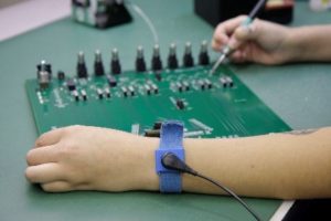
ESD Negative Effect on Reverse Engineering Printed Circuit Board
Reverse engineering printed circuit board need to take the ESD negative effect into consideration, ESD from human body, environment as well as electronic device itself will bring damage to the semiconductor and microcontroller such as penetrate the thin isolation layer in the internal part of electronic components; damage the grid in the MOSFET & CMOS; lock the trigger in the cmos components;
ESD Negative Effect on Reverse Engineering Printed Circuit Board
Melt down the soldering or aluminum wire inside the active device. In order to eliminate the interference and damage generated from ESD device, multiple measures must be taken:
1. Ensure each one circuit should as close to each other as possible;
2. PUT all the connector together as close as possible;
3. introduce the wire from the center of printed circuit board if possible, and keep away from the area which can be affected by ESD directly;
4. wide cabinet or polygon filled stuff must be placed underneath all of the Printed circuit board layers where is more susceptible to get affect by ESD;
5. place the tool holes in the rim of printed circuit board, around the hole use pad from top layer and bottom layer of printed circuit board without solder resist to connect them to the cabinet;
6. when assemble printed circuit board, don’t print any solder tin on the pads of top and bottom layer, use the screw with internal embed gasket to practice the internal attachment with cabinet shielding layer or the fixture on the ground;
7. reverse engineering similar isolated area on each layer of cabinet layer and circuit layer; keep the space as 0.64mm if possible;
8. Connect cabinet grounding and circuit ground through the 1.27mm alongside the cabinet ground track each 100mm where is close to the tool holes location in the top and bottom layer of PRINTED CIRCUIT BOARD. These grounding track can be cut off by a knife or keep it as open circuit. Use magnetic bead or high frequency capacitor to jump the PCB Reverse Engineering.
Tags: reverse engineering circuit board,reverse engineering circuit card,reverse engineering pcb,reverse engineering pcb assemble,reverse engineering pcb board,reverse engineering pcb card,reverse engineering pcba,reverse engineering printed circuit board,reverse engineering printed wiring board,reverse engineering pwb,reverse engineering pwba