

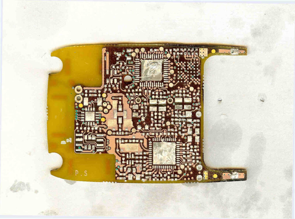
Reverse Engineering Printed Circuit Board Grounding
Reverse Engineering Printed Circuit Board grounding layer and power layer can extract gerber file, restore schematic diagram and compiling bill of material;
Reverse engineering PCB need to consider the depressing of power supply line and grounding line impedance, when design the Printed Circuit Board with high density of assembly point, it is critical to consider decreasing the power supply line and grounding line impedance, necessary measures must be taken on the common impedance/cross-talk and reflection generated from wave distortion and osillation phenomenon.
There are too much integrated circuit parts working simutaneously on the Printed Circuit Board cloning, power supply voltage and ground electrical level could fluctuated easily and cause the signal oscillation and mis-operation. Especially when the surge current flow through the Printed Circuit Board tracks, it will show the existence of transcient voltage decreasing and cause the power supply peak noice, which is dominated by the conductor conductance interference.
When clone PCB circuit board layout design, should avoid the effect of circuit on the conductance as much as possible: connect the side-way capacitor among the each integrated circuit power supply and grounding lines, to shorten the through route in the switch current; design the power supply line and ground line into the grid shape instead of comb shape, since grid shape can effectively shorten the circuit loop and decrease the circuit impedance and interference.
Tags: replicate circuit board,replicate circuit card,replicate pcb,replicate pcb assemble,replicate pcb board,replicate pcb card,replicate pcba,replicate printed circuit board,replicate printed wiring board,replicate pwb,replicate pwba