"Everything we build starts with design engineering. CECL manufactured boards for one of our products. It went perfectly – a real success.It is really an high quality service they have provided to us!"
By Nile Smith from Sinotech Inc.
“We had several very old device with obsolete boards need to be replaced –through CECL professional service.We got what we needed, and we’ve been using the results of the work without any problem till now.”
By Richard Anderson from TWP system Inc.
"Guys from CECL manufacture PCBs we use in one of our products, a clinometer and we’ve never had a problem with anything. The boards come in, they work. And, their team is very responsive."
Per i prodotti elettronici ad alta velocità e ad alta frequenza, la retroingegneria dello schema di layout PCB per il test di impedenza richiede un livello di verifica considerevolmente superiore rispetto alla normale ricostruzione di una PCB. Quando una PCB contiene piste con impedenza controllata, l’obiettivo non è semplicemente riprodurre il percorso visibile delle piste in rame, ma recuperare nel modo più accurato possibile le caratteristiche elettriche del progetto originale. Le coppie differenziali, le linee di segnale ad alta velocità, i percorsi di trasmissione RF, le interfacce USB, i canali PCIe, le connessioni Ethernet e altri circuiti sensibili possono dipendere da una specifica larghezza delle piste, dalla distanza tra le piste, dallo spessore del dielettrico, dallo spessore del rame e dalla configurazione degli strati. Pertanto, lo schema elettrico, il file PCB, il file Gerber, la lista BOM e gli altri documenti di progettazione recuperati devono essere verificati e confrontati tra loro prima della produzione di una PCB riprodotta.
– minimum of 1 inch (Tektronix*/Hewlett Packard*).
· Microstrip structures must provide signal and reference plane pads.
· Stripline structures must provide a signal pad and a pad for each reference plane.
· Pads for handheld probes should be a minimum of 0.025 inches in diameter with 100 to 150 mils(2.54 to 3.81mm) spacing between signal and ground.
· Microprobe pad dimensions are shown in the following section.
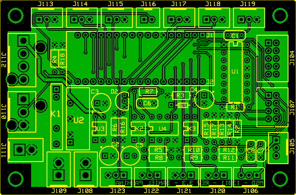
Reverse Engineering PCB Layout Scheme from physical Printed circuit board target can provide great convenience for Impedance Test in the upcoming PCB card cloning and PCB re-manufacturing process
Para productos electrónicos de alta velocidad y alta frecuencia, la ingeniería inversa del esquema de diseño de PCB para pruebas de impedancia requiere un nivel de verificación considerablemente superior al de una reconstrucción convencional de PCB. Cuando una PCB contiene pistas con impedancia controlada, el objetivo no consiste simplemente en reproducir el trazado visible de cobre, sino en recuperar con la mayor precisión posible las características eléctricas del diseño original. Los pares diferenciales, las líneas de señal de alta velocidad, las rutas de transmisión de RF, las interfaces USB, los canales PCIe, las conexiones Ethernet y otros circuitos sensibles pueden depender de un ancho de pista específico, una separación determinada, un espesor dieléctrico concreto, un espesor de cobre definido y una configuración específica de capas. Por lo tanto, el diagrama esquemático, el archivo PCB, el archivo Gerber, la lista BOM y los demás documentos de ingeniería recuperados deben compararse y verificarse de forma cruzada antes de fabricar una PCB reproducida.
Para produtos eletrônicos de alta velocidade e alta frequência, a engenharia reversa do esquema de layout de PCB para teste de impedância exige um nível de verificação consideravelmente mais elevado do que uma reconstrução convencional de PCB. Quando uma PCB contém trilhas com impedância controlada, o objetivo não é simplesmente reproduzir o roteamento de cobre visível, mas recuperar com a maior precisão possível as características elétricas do projeto original. Pares diferenciais, linhas de sinal de alta velocidade, caminhos de transmissão de RF, interfaces USB, canais PCIe, conexões Ethernet e outros circuitos sensíveis podem depender de uma largura específica de trilha, espaçamento entre trilhas, espessura do dielétrico, espessura do cobre e configuração das camadas. Portanto, o diagrama esquemático, o arquivo PCB, o arquivo Gerber, a lista BOM e outros documentos de engenharia recuperados devem ser verificados e comparados entre si antes que uma PCB reproduzida seja fabricada.
The resulting Gerber file should be independently reviewed layer by layer rather than assuming that a correct PCB file automatically guarantees correct manufacturing data. Copper layers, solder masks, drill files, board outlines, and critical routing should be compared with the original PCB. For multilayer boards, impedance calculations or field-solver analysis can be used to estimate whether the reconstructed geometry is capable of achieving the intended characteristic impedance.
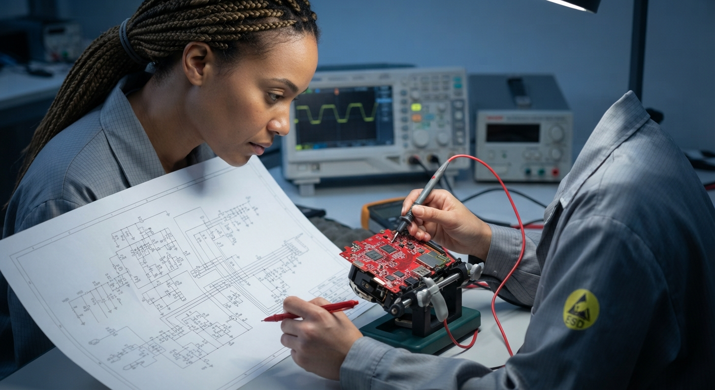
After the documentation has been verified, impedance testing of the prototype PCB provides an important physical validation step. A prototype can be manufactured using the recovered Gerber data and the proposed PCB stack-up, followed by controlled-impedance testing with suitable test equipment such as a time-domain reflectometer (TDR). Depending on the application, engineers may test single-ended impedance and differential impedance at selected test coupons or representative signal structures.
Pour les produits électroniques à haute vitesse et à haute fréquence, la rétro-ingénierie du schéma de routage PCB pour les tests d’impédance exige un niveau de vérification considérablement plus élevé qu’une reconstruction classique de PCB. Lorsqu’une PCB comporte des pistes à impédance contrôlée, l’objectif n’est pas simplement de reproduire le routage visible en cuivre, mais de récupérer aussi précisément que possible les caractéristiques électriques de la conception d’origine. Les paires différentielles, les lignes de signaux à haute vitesse, les chemins de transmission RF, les interfaces USB, les canaux PCIe, les connexions Ethernet et autres circuits sensibles peuvent dépendre d’une largeur de piste spécifique, d’un espacement précis, d’une épaisseur de diélectrique donnée, d’une épaisseur de cuivre déterminée et d’une configuration particulière des couches. Par conséquent, le schéma électrique, le fichier PCB, le fichier Gerber, la nomenclature BOM et les autres documents d’ingénierie récupérés doivent être vérifiés et comparés entre eux avant la fabrication d’une PCB reproduite.
Measured results can then be compared with the target impedance and the expected values calculated from the reconstructed PCB design. If significant differences appear, the investigation should determine whether the cause is incorrect trace geometry, PCB material variation, stack-up deviation, copper thickness, fabrication tolerance, or an error in the reverse-engineered layout.
Voor elektronische producten met hoge snelheid en hoge frequentie vereist reverse engineering van het PCB-layoutschema voor impedantietests een aanzienlijk hoger verificatieniveau dan een gewone PCB-reconstructie. Wanneer een PCB sporen met gecontroleerde impedantie bevat, is het doel niet alleen om de zichtbare koperen routing te reproduceren, maar ook om de elektrische eigenschappen van het oorspronkelijke ontwerp zo nauwkeurig mogelijk te reconstrueren. Differentieelparen, hogesnelheidssignaallijnen, RF-transmissiepaden, USB-interfaces, PCIe-kanalen, Ethernetverbindingen en andere gevoelige schakelingen kunnen afhankelijk zijn van een specifieke spoorbreedte, spoorafstand, diëlektrische dikte, koperdikte en laagconfiguratie. Daarom moeten het gereconstrueerde schema, het PCB-bestand, het Gerber-bestand, de BOM-lijst en andere engineeringdocumenten onderling worden gecontroleerd en vergeleken voordat een gereproduceerde PCB wordt vervaardigd.
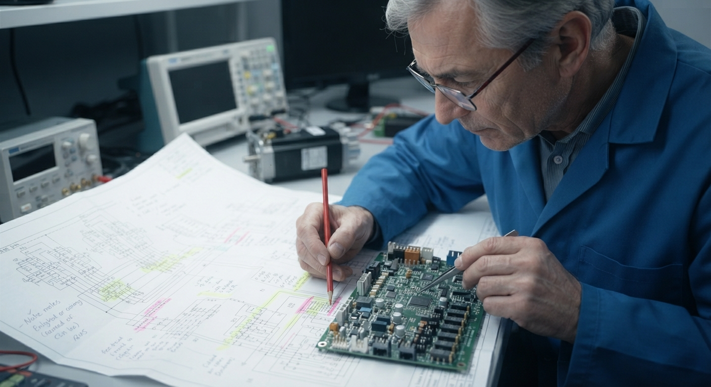
A reliable reverse engineering PCB layout scheme for impedance test therefore combines document verification, electrical reconstruction, simulation, prototype fabrication, and physical measurement. The schematic diagram establishes signal relationships, the BOM list confirms component information, the PCB file defines the physical design, and the Gerber file represents the manufacturing output.
Für elektronische Produkte mit hoher Geschwindigkeit und hohen Frequenzen erfordert das Reverse Engineering eines PCB-Layoutkonzepts für Impedanztests ein wesentlich höheres Maß an Verifizierung als eine gewöhnliche PCB-Rekonstruktion. Wenn eine PCB impedanzkontrollierte Leiterbahnen enthält, besteht das Ziel nicht lediglich darin, die sichtbare Kupferführung zu reproduzieren, sondern die elektrischen Eigenschaften des ursprünglichen Designs so genau wie möglich wiederherzustellen. Differenzielle Leitungspaare, Hochgeschwindigkeitssignalleitungen, HF-Übertragungswege, USB-Schnittstellen, PCIe-Kanäle, Ethernet-Verbindungen und andere empfindliche Schaltungen können von einer bestimmten Leiterbahnbreite, einem definierten Leiterbahnabstand, einer bestimmten Dielektrikumsdicke, einer festgelegten Kupferdicke und einer spezifischen Lagenkonfiguration abhängen. Daher müssen der rekonstruierte Schaltplan, die PCB-Datei, die Gerber-Datei, die BOM-Liste und weitere technische Unterlagen vor der Herstellung einer reproduzierten PCB miteinander abgeglichen und überprüft werden.
By correlating these documents and validating the final prototype through impedance measurement, engineers can identify errors before mass production and improve the accuracy and preciseness of the reverse-engineered PCB. This methodology is particularly valuable when reproducing legacy high-speed boards for which the original CAD files, stack-up information, or manufacturing documentation are no longer available.