

Reverse Engineering PCB Assemble
Reverse Engineering PCB Assemble need to make the BOM on which the footprint of each component will be specified as well as the necessary description and depictorial explanation if it is possible.
Now in order to find the footprint for this package we will open the library manger, and open the footprint library called SOG. The SOG library will have many of the footprints for the most common SMT IC’s we use in our designs (SOIC, TSSOP, etc.). In the SOG library there is a list of different footprints and the differences may be very slight. The distance between two adjacent pins is called the pitch, and this is a very important value.
Reverse Engineering PCB Assemble
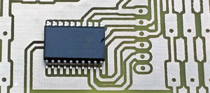
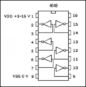
You may see a footprint with the name SOG.050/18/WG.350/L.550. What this means is that the pitch is .050 inches, the number of pins is 18, the gull width or the width from one pin end to another is .350 inches, and the length is about .550 inches. Let’s now pick a footprint for the inverter IC which we have chosen. You can see that the pitch is .050, the number of pins is 14, the gull width is about .244, and the length is about .344.
Therefore the footprint we can use is, SOG.050/14/WG.244/L.350. The length is the only value that does not have to be exact. Just pick a footprint length that is the next larger then the IC itself. This is an image of the corresponding footprint chosen for the inverter IC.
invertor IC image
There are instances when a footprint for your IC package may not exist. If this happens a footprint must be made according to the specifications on the data sheet. To start this process, click on the “Create New Footprint” button in the library manager. A popup box will ask you for the name of the component, and the units required. Click on the units specified for the footprint (Note: This is normally going to be English. The unit mils stand for one millionth of an inch, NOT millimeters).
Next, if you are making the footprint for an IC, you can Use the “Pad Array Generator”, otherwise just press “OK”. If you are using the “Pad Array Generator”, then put in the parameters needed to make the pad. You will now see a circle in the center of your black screen. This circle represents a “Pad” which is the way in which one pin will be mounted to your PCB. Depending on which component we are designing, this pad may have to be changed after Reverse Engineering PCB Assemble.
Tags: reverse engineering circuit board,reverse engineering circuit card,reverse engineering pcb,reverse engineering pcb assemble,reverse engineering pcb board,reverse engineering pcb card,reverse engineering pcba,reverse engineering printed circuit board,reverse engineering printed wiring board,reverse engineering pwb,reverse engineering pwba