

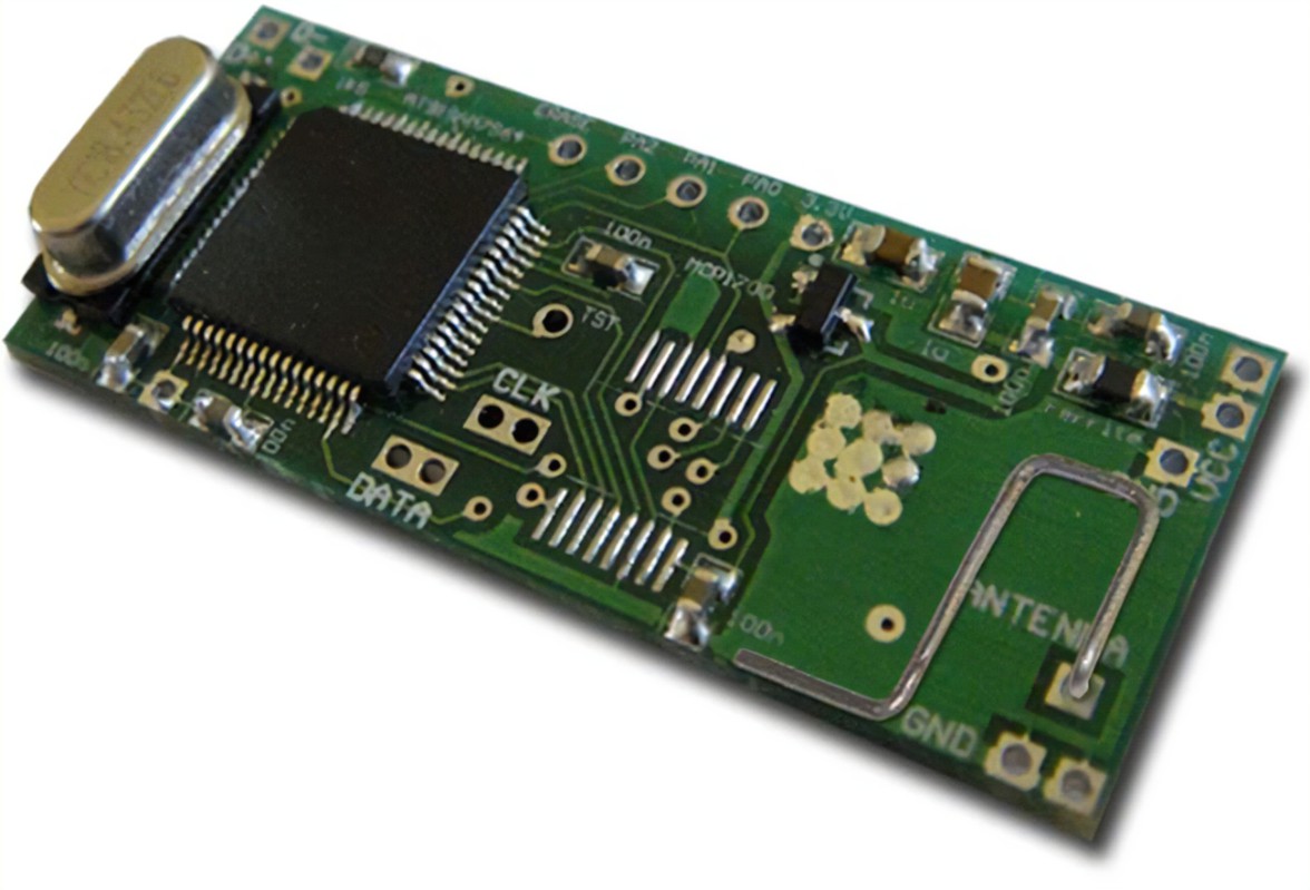
Reverse Engineering Micro-controller PCB Board
The most basic process of Reverse Engineering Micro-controller PCB Board can be divided into three steps: cloning of the circuit board schematic diagram, the generation of the net-list, and the design of the printed circuit board gerber file and layout drawing.
Whether it is the device layout or wiring on the pc board, there are specific requirements; For example, the input and output traces should be avoided as much as possible to avoid interference. The parallel wiring of the two signal lines must be isolated by the ground wire, and the wiring of the two adjacent layers should be perpendicular to each other as much as possible, and it is easy to cause parasitic coupling in parallel.
The power and ground wires should be divided into two layers perpendicular to each other as much as possible. In terms of line width, a wide ground wire can be used as a loop for the digital circuit PCB, that is, a ground network (analog circuits cannot be used in this way), and a large area of copper is used.
The following article explains the principles and details that need to be paid attention to in the PCB reverse engineering of the single-chip control board. In terms of the layout of components, the related components should be placed as close as possible.
For example, the clock generator, crystal oscillator, and the clock input of the CPU are prone to noise, so they should be placed closer. For those devices that are prone to noise, small current circuits, high current circuit switching circuits, etc., it should be kept away from the logic control circuit and storage circuit (ROM, RAM) of the single-chip microcomputer as far as possible. If possible, these circuits can be made into circuits board, which is conducive to anti-interference and improves the reliability of reverse engineering micro-controller pcb board system;