

Reverse Engineering Control Board Wiring Diagram
Reverse Engineering Control Board Wiring Diagram, you can clearly see where there may be a problem. The analog trace in the picture is connected from the tap of U3a to the high impedance input of U4a amplifier.
The digital trace in the figure conveys the digital code for programming the digital potentiometer settings. After measuring on the test board, it is found that the digital signal in the digital trace is coupled to the sensitive analog trace, see below Figure.
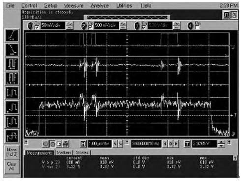
(Noise on adjacent analog traces), the bottom waveform is taken from TP10 (Noise on 16-bit D/A converter output)
The digital signal programmed to the digital potentiometer in the system is gradually transmitted along the trace to the analog line that outputs the DC voltage. This noise propagates through the analog part of the circuit to the third digital potentiometer (U5a).
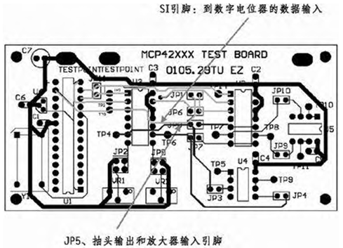
The third digital potentiometer toggles between the two output states. The main solution to this problem is to separate the traces. below Figure shows an improved wiring scheme.
After carefully separating the analog and digital traces, the circuit becomes a very “clean” 16-bit D/A converter. The waveform in the figure is the single-code conversion result of the third digital potentiometer, 76.29mV.
After the digital and analog design ranges are determined, careful PCB card layout is essential to a successful PCB. Especially when active digital traces are close to high-impedance analog traces, they will cause severe coupling noise, which can only be avoided by increasing the distance between traces.