

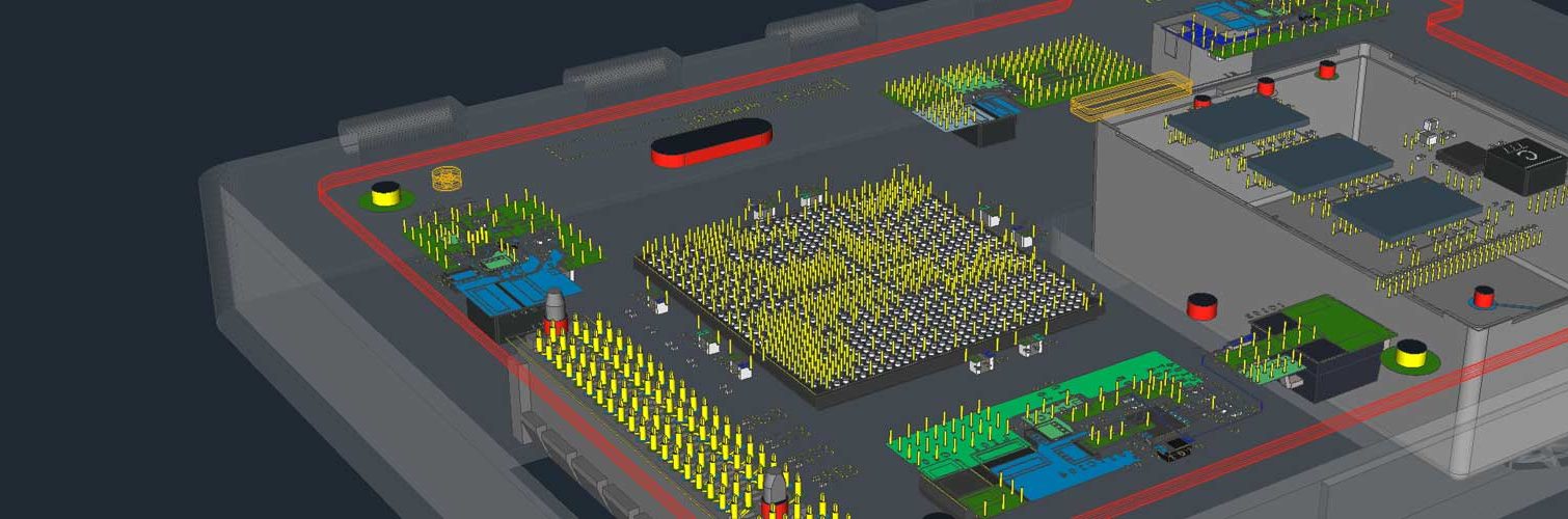
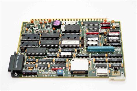
Reverse Engineering Automation PCB Board Schematic Diagram
When Reverse Engineering Automation PCB Board Schematic Diagram, we often rely on previous experience and tips found online. Some rules are general in PCB electronic board designing, and some rules can only be used in a specific printed circuit board reverse engineering design.
For example, the rules for analog-to-digital converter PCBs do not apply to RF, and vice versa. However, certain guidelines can be considered universal for any printed circuit board reverse engineering. Let’s take a look today at some methods and techniques that can significantly improve the basic issues of PCB design.
Power and Signal Distribution
Power distribution is a critical element in any Reverse Engineering Automation PCB Board Schematic Diagram. All components rely on power to function.
Depending on your design, some components may have better power connections and some components on the same board may have poorer power connections.

For example, if all components are powered by a single trace, each component will observe a different impedance, resulting in multiple ground references. For example, if you have two ADC circuits, one at the beginning and the other at the end, and both ADCs read an external voltage, each analog circuit will read a different potential relative to their own.