

Reverse Engineer Circuit Board Power/Ground/Signal Layout Pattern
After placing the components, the job will enter the process of Reverse Engineer Circuit Board Power/Ground/Signal Layout Pattern, you can place power, ground, and signal traces to ensure that your signal has a clean and trouble-free path.
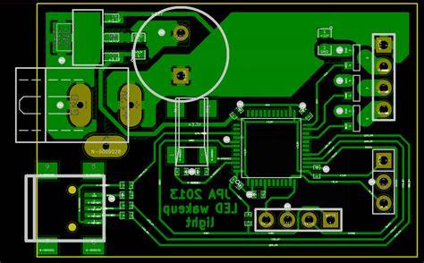
At this stage of printed wiring board reverse engineering process, keep the following guidelines in mind:
1) Locate the power and ground plane layers
It is always recommended to place the power and ground plane layers inside the circuit board while maintaining symmetry and centering. This helps prevent your circuit board from bending, which is also related to the correct positioning of your components.
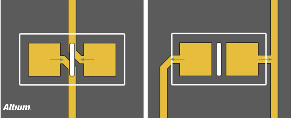
For supplying power to the Integrated circuit, it is recommended to use a common channel for each power supply to ensure a solid and stable trace width, and avoid component-to-component daisy chain power connections.
2) Signal wire re-routing connection
Next, connect the signal wires according to the redesign in the PCB board schematic. It is recommended to always take the shortest possible path and direct path between components.
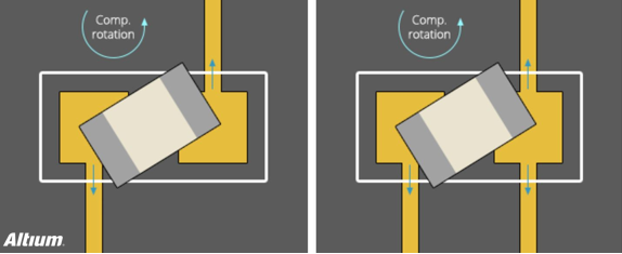
If your components need to be fixed and placed in the horizontal direction without deviation, it is recommended to re-route the PCB circuit board wires basically horizontally where the components of the circuit board exit, and then perform vertical wiring after the exit.
In this way, as the solder moves during soldering, the component will be fixed in the horizontal direction. As shown in the upper part of the figure below. The signal routing method in the lower half of the figure below may cause component deflection as the solder flows during soldering.