


Reverse ATMEL Locked AT89S8252 MCU Program
Reverse ATMEL Locked AT89S8252 MCU Program needs to and ;
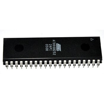
The DSP engine, dual 40-bit accumulators, hardware support for division operations, barrel shifter, 17 x 17 multiplier, a large array of 16-bit working registers and a wide variety of data addressing modes, together provide the AT89S8252 Central Processing Unit (CPU) with extensive mathematical processing capability.
Flexible and deterministic interrupt handling, coupled with a powerful array of peripherals, renders the AT89S8252 devices suitable in the layer contrl for pcb card assemble cloning. Further, Direct Memory Access (DMA) enables overhead-free transfer of data between several peripherals and a dedicated DMA RAM. Reliable, field programmable Flash program memory ensures scalability of applications that use AT89S8252 devices.
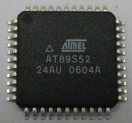
Figure 1-1 illustrates a general block diagram of the various core and peripheral modules in the AT89S8252 family of devices. Table 1-1 provides the functions of the various pins illustrated in the pinout diagrams.
Getting started with the AT89S8252 MCU family of 16-bit Digital Signal Controllers (DSCs) requires attention to a minimal set of device pin connections before proceeding with development. The following is a list of pin names, which must always be connected: