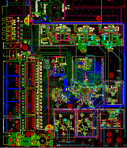
Redrawing PCB Board Layout Diagram to reduce Electronic Magnetic Interference
The three major elements of EMC, interference sources, transmission channels and sensitive devices. Therefore, Redrawing PCB Board Layout Diagram to reduce Electronic Magnetic Interference starts with eliminating interference sources, cutting off the propagation path and shielding sensitive devices. The following methods are considered based on these ideas.
Reasonable relayout electronic pcb card circuitry scheme
In terms of PCB Board circuitry pattern design, in principle, devices related to each other should be placed as close as possible, digital circuits, analog circuits, and power circuits should be placed separately, and high-frequency circuits should be separated from low-frequency circuits.
Noise-prone devices, low-current circuits, and high-current circuits should be kept away from logic circuits as much as possible. Main interference and radiation sources such as clock circuits and high-frequency circuits should be arranged separately and far away from sensitive circuits.