Redesign Printed Circuit Board Schematic Diagram
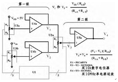
Redesign Printed Circuit Board Schematic Diagram make this circuit wiring diagram have the performance of a 16-bit D/A converter, a third digital potentiometer (U2a) is used across the output terminals of the two operational amplifiers (U4a and U4b).

U3a and U3b are programmed to set the voltage value after the digital potentiometer. If VDD is 5V, the output of U3a and U3b can be programmed to differ by 19.61mV.
This voltage is passed through the third 8-bit digital potentiometer R3, and the LSB of the entire circuit from left to right is 76.3mV. The stringent device specifications required for this circuit to achieve optimal performance.
This circuit has two basic operating modes. The first mode can be used to obtain a programmable and adjustable DC differential voltage.
In this mode, the digital part of the circuit is only used occasionally and is not used during normal operation. The second mode is to use this circuit as an arbitrary waveform generator.
In this mode, the digital part of the circuit is an essential part of the circuit operation. The danger of capacitive coupling may occur in this mode.
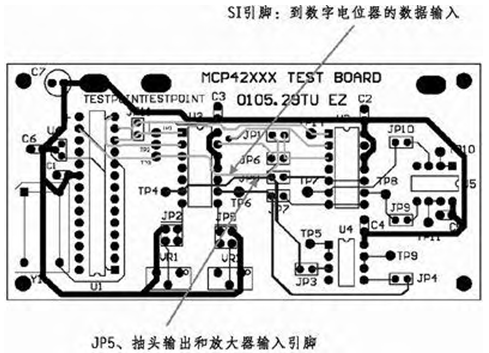
The first wiring of the circuit shown in below Figure. This printed circuit board layout was quickly redesigned in the laboratory without paying attention to details. When checking the wiring, it was found that the digital wiring was placed next to the high-impedance analog circuit.
It should be emphasized that the wiring should be correct the first time. The purpose of this article is to explain how to identify problems and how to make major improvements to the electronic pcb card layout.