

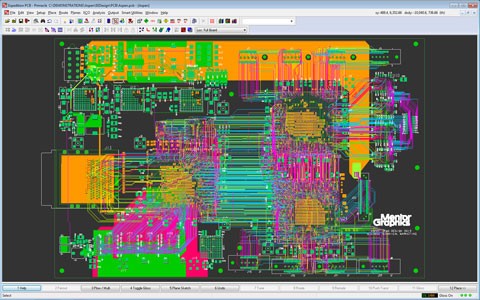
Redesign PCB Board Layout Diagram Procedures
Redesign PCB Board Layout Diagram is a reverse engineering process which will start from desolder electronic/mechanical components off the PC board, and then we are going to require design components on the newly cloned PCB layout drawing,
1, Use Schematic design tool to draw it then generate corresponded net-list, of course in the special circumstance such as a simple PCB board, there is no need to carry out the schematic drawing designing if the net-list has existed, enter directly into the PCB design system, in the system can pick up the component footprint directly to generate net-list manually.
2, Change the net-list manually, define the fixed pin on the components which has been designed on the soldering pad of schematic diagram, for those pins without any physical connection can lead to the ground or protection ground, etc. categorize the pins with different names with schematic and PCB footprint align with the PCB library especially the diode, transistor, etc.