PWB Clone Over Grounding Line Noise
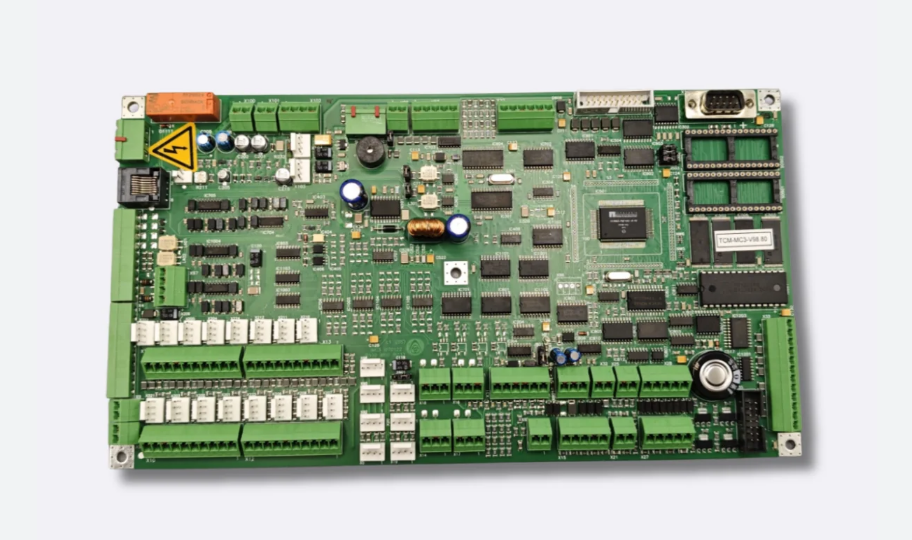
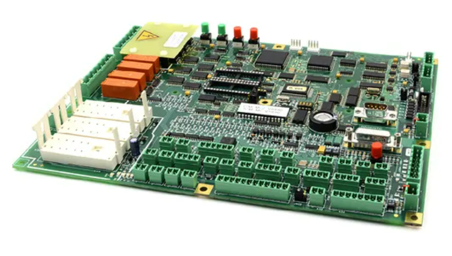
Cloning a printed wiring board used in a Transmission Control Module (TCM) requires careful attention to grounding structure and line noise control. In a backhoe loader, the TCM PCB governs automatic gear shifting and torque distribution, coordinating signals between sensors, hydraulic actuators, and the vehicle control network. Because these systems operate in a high-current, high-vibration environment, grounding noise can significantly influence signal accuracy and communication stability. During PWB clone projects, engineers must do more than simply copy copper traces; they must recover the electrical intention behind grounding planes, filtering networks, and signal reference paths. Reverse engineering techniques allow engineers to restore circuit logic and recreate the original behavior while ensuring that the reproduced board maintains stable gear-shift timing and torque control.
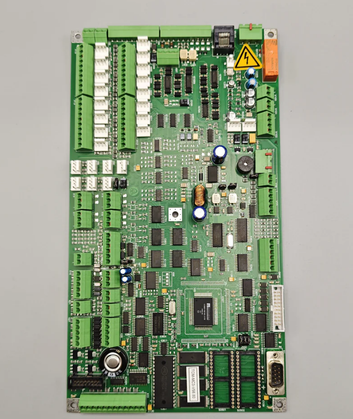
A key stage in addressing grounding line noise during PWB clone is the reconstruction of technical documentation. Engineers carefully analyze the original board to recover the schematic diagram, netlist, layout drawing, and Gerber file that define the PCB structure. Each trace and via is inspected to recreate ground return paths and signal isolation areas that prevent interference between power circuits and digital control lines. The bom list is also rebuilt to verify the values of decoupling capacitors, ferrite beads, and filtering components used to suppress noise. During reverse engineering, the recovered netlist is compared with the schematic diagram to ensure electrical consistency before attempting to clone or duplicate the PCB. Once validated, the layout drawing and Gerber file can be used to reproduce the board accurately. This dense documentation process ensures that engineers do not simply replicate visual features but restore the functional integrity of the TCM circuitry.
Grounding Line Noise is a commonly issue when design PCB board schematic diagram, PWB Clone will inevitably encounter the noise issue from power supply line, when the emergence of electro-magnetic interference on the digital circuit, the main reason is on the power supply line and grounding line, use oscillograph to monitor the obvious noise voltage.
Although there are a lot of people can assure that these noises is the main cause for electro-magnetic interference when PWB clone, but normally has no effective measures to deal with them, in order to achieve the purpose of noise elimination, it is necessary to understand the generating source of these noises:
Noise on the grounding line, when the occurrence of peak current from the power supply line, there is also some current flow through the grounding line, especially when the output electrical level turns from high to low for Clone Signal Amplifier PCBA, and the peak current from the ground line could be higher.
Due to the different conductance value on the grounding line which can also generate the voltage, and cause the grounding noise. The noise on the grounding line and power supply line can not only make the operation efficiency of circuit lower, but also generate stronger electro-magnetic radiation.
ICC means current on the power supply: when in the different output status, the radiation range is different. When the status is steady, so as the current will be steady. When the output switch from low to high status, and transient short circuit for increasing current, meanwhile the parasite capacitance will be charged for larger current; when output voltage switch from high to low for PWB clone, transient short circuit happen to increase the current, it will not charge the capacitance, so the current output will switch from low to high electrical level. VCC voltage on the power supply: when the ICC happens to mute, the conductance on the power supply line will generate conductive voltage; Grounding line current, when output from the power supply and parasite capacitance charge to form the current with steady output and steady current.
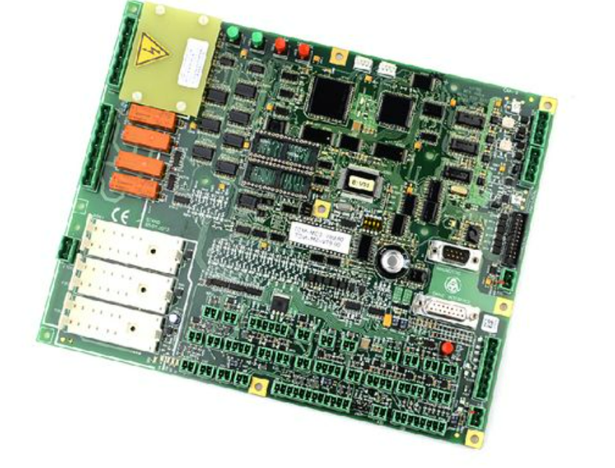
Grounding optimization is another important technical focus when engineers replicate or refurbish the PWB. During reverse engineering analysis, specialists examine whether analog sensor inputs, communication interfaces, and high-current driver circuits share common ground regions or require isolated return paths. In many cases, controlled redesign or redevelopment may improve noise suppression while maintaining electrical compatibility with the original system. By studying the recovered schematic diagram and netlist, engineers can identify ground loops, switching noise sources, and potential electromagnetic coupling paths. The recreated layout drawing may therefore include refined grounding strategies, such as improved plane segmentation or enhanced decoupling placement. While these changes remain faithful to the original architecture, they help ensure that the reproduced TCM board delivers stable automatic shifting and torque distribution performance under demanding operating conditions.
The final stage of the PWB clone process involves prototype validation and preparation for remanufacture. Once engineers restore all documentation—including the schematic diagram, bom list, netlist, layout drawing, and Gerber file—prototype PCBs are fabricated to confirm performance. Electrical testing verifies that the duplicated board communicates correctly with sensors and actuators while maintaining low noise levels across grounding networks. Environmental testing, such as vibration and temperature cycling, ensures that the remanufactured board can withstand the harsh environment of backhoe loader operations. Through careful reverse engineering, disciplined documentation recovery, and strategic grounding analysis, organizations can confidently reproduce and replicate TCM printed wiring boards. This systematic cloning approach ensures reliable transmission control while also supporting refurbishment and long-term redevelopment of heavy machinery electronics.