

Reverse Engineering PCB Process Variation
In the field of electronics restoration, Reverse Engineering PCB Process Variation refers to the adjustments and adaptations engineers must make when recovering, reproducing, or replicating a printed circuit board (PCB) from limited or damaged resources. Unlike a standardized production workflow, reverse engineering is often influenced by the condition of the original sample, the complexity of the design, and the intended application of the recreated board. Understanding these variations is key to restoring lost Gerber files, schematic diagrams, layout drawings, BOM lists, and netlists for obsolete or phase-out PCB assemblies.

Understanding Process Variation in PCB Reverse Engineering
The reverse engineering process for a PCB typically begins with recovering and restoring the design from a physical sample. However, no two projects are exactly alike. Process variation can occur due to:
- Board Condition – An aged or partially damaged board may require additional inspection steps or reconstruction of missing layers.
- Technology Differences – High-frequency, multi-layer boards demand more precision than simple single-layer designs.
- Component Availability – Discontinued components may necessitate substitutions and redesign of specific circuits.
- End Application Requirements – A PCB for medical equipment may require higher compliance standards compared to a consumer device.
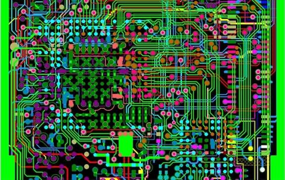
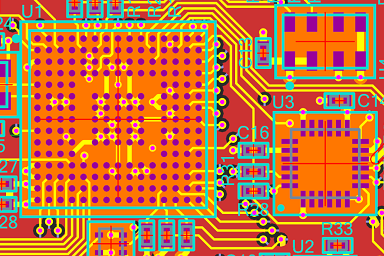
These variations mean that the workflow may involve extra scanning techniques, manual tracing of copper tracks, or in some cases, advanced imaging methods to extract hidden inner layers.
The Workflow: From Physical Board to Recreated Documents
A typical Reverse Engineering PCB Process Variation might proceed as follows:
- Initial Assessment – Evaluating board structure, layer count, and identifying damaged or missing regions.
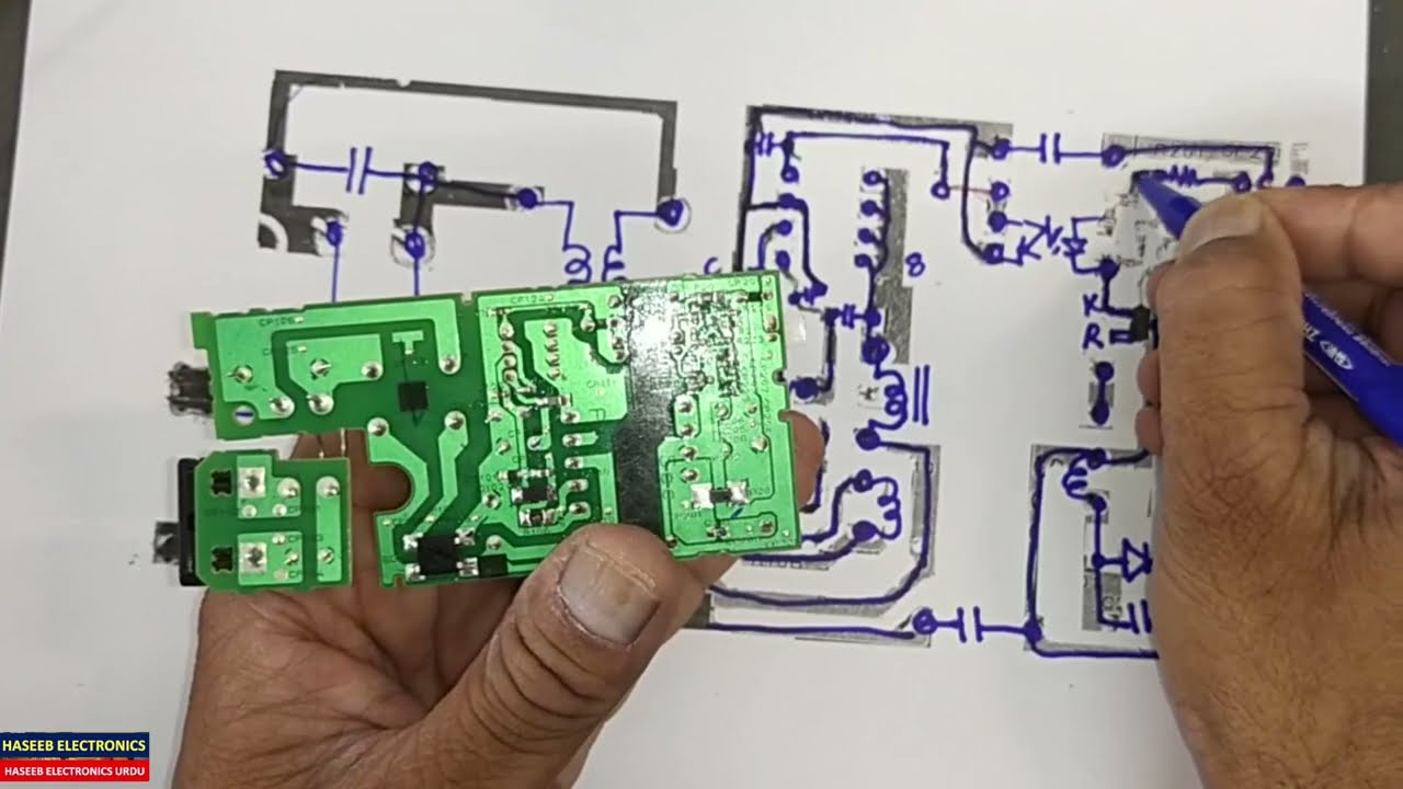
- Data Capture – Using precision scanning or microscopic imaging to recreate accurate layout drawings.
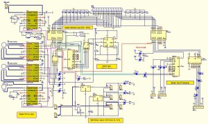
- Schematic Recreation – Translating the captured data into a clear schematic diagram for circuit understanding.
- BOM Recovery – Identifying and documenting components, then building a complete BOM list.
- Netlist Generation – Verifying electrical connections to ensure functional accuracy.
- Output Creation – Producing Gerber files and manufacturing-ready documents.
This process can be repeated with adjustments depending on the level of detail available and the functional requirements of the target product.
Applications in Industry
Restored PCB data from this process variation is especially valuable for industries where certain equipment remains in service long after production has ended. Common examples include:
- Industrial control systems – where replacing the entire machine is impractical.
- Aerospace and defense electronics – requiring exact duplication or cloning for mission-critical systems.
- Medical diagnostic devices – where redevelopment is essential to maintain compliance while keeping the original functionality.
- Specialized consumer products – such as professional audio gear or legacy gaming systems.
In all these cases, the ability to recreate obsolete designs ensures operational continuity without costly redesigns from scratch.
Strategic Value to Companies and Individuals
For a company, engaging in Reverse Engineering PCB Process Variation offers the advantage of preserving investment in proven products while extending their lifecycle. For individuals or small businesses, it’s an affordable way to refurbish or remanufacture discontinued boards for repairs or upgrades. This service restores control over critical technical data, enabling faster maintenance, cost-effective reproduction, and future redevelopment opportunities.
Conclusion
Reverse engineering is never a one-size-fits-all process. Reverse Engineering PCB Process Variation ensures that each project is tailored to the specific conditions of the existing board and the needs of its end application. Whether the goal is to restore lost documentation, replicate a phase-out PCB, or duplicate a specialized product board, process variation makes it possible to adapt and deliver results that meet both performance and reliability standards.
Process variation when reverse engineering PCB is a comonly situations in which lots of projects will experienced. During which manufacturing process variation is the most frequently seen variation and can produce some strange numbers for part or assembly dimensions. Unless the dimensions or specifications for the next higher assembly are known, “normalizing” of interface dimensions is not recommended.