

Printed Wiring Board Reverse Engineering Obstacle Tool
This is the Printed Wiring Board Reverse Engineering Obstacle tool. Right click and select new, right click again and click on properties. The Edit Obstacle screen will appear as shown in Fig. 11.
Change the obstacle type to place outline. The obstacle layer should be changed to Global, and then click ok. Next, click and drag your box until it resembles the component made. This will show the outline of where the component is on the board. This also makes sure that you do not place components over one another. The finished power connector is in below Figure:
Save the footprint into a directory by selecting “Save As”. I like to save all of my footprints into a directory labeled “MYFOOTPRINTS”. It is a good idea to print the component package, make sure that the pins align correctly with your actual component before manufacture PCB board. To do this we print the PCB board layout, and line up the pads to the pins. Printing will be demonstrated later after PCB Board Reverse Engineering is complete.
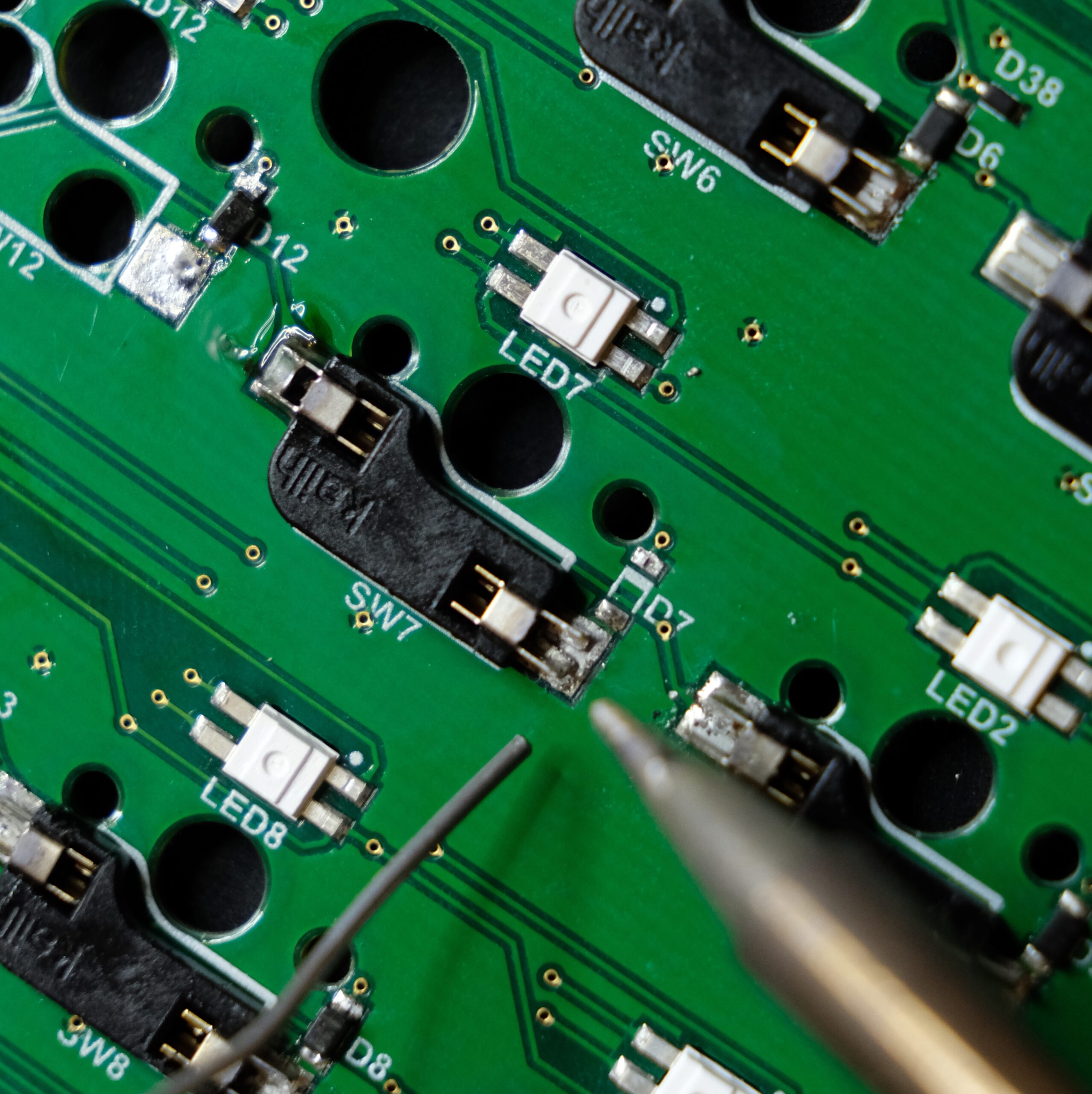
So far in this tutorial, you have learned how to make your PCB design in Capture, and make the footprints for each component. It is now time to transfer your design into Layout, and begin reverse engineering printed wiring board.
Tags: flexible pcb card reverse engineering,pcb assemble reverse engineering,pcb board reverse engineering,pcb card reverse engineering,pcb reverse engineering,pcba reverse engineering,Printed Circuit Board Reverse Engineering,printed wiring board reverse engineering,pwb reverse engineering,pwba reverse engineering