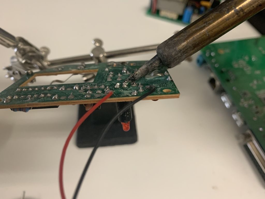
Printed Circuit Card Reverse Engineering
Printed Circuit Card Reverse Engineering can help restore the circuitry scheme file and schematic diagram from original PCB board which has been out of the market and too obsolete to be found;

Drill and plating are two of the most important aspects of manufacture after electronic pcb board Reverse Engineering, when produce the Printed circuit card with multilayer, especially when there is buried or blind vias inside its internal structure, before each one of these internal layer pressed, it is necessary to get them drilled and plated. If this process hasn’t been completed properly, it will not be able to interconnect them.
According to the drilling requirement, the hole wall must be treated by the plated through hole treatment. After the hole wall has become metallic, can use the internal circuit layers interconnect each other for multilayer Printed circuit card, as a matter of fact, inner layer circuitry pattern is one of the most difficult part to make when reverse engineering printed circuit board gerber file. Before the start of electrical plating, the residual inside the hole wall must be removed. That is because epoxy glass and resin can have chemical alteration after heating and cover the internal part of Printed circuit card layer, so it is necessary to remove them first and this process will be done in the chemical process.
Multilayer Printed circuit card Lamination
Several single Printed circuit card layer must be pressed to manufacture the multilayer Printed circuit card. this action includes to add the insulation layer among them, and make them attach to each other better, etc. if there is vias which require to go through several layers, then each layer must be treated for several times. The layout and image transfer of top and bottom layer will be done after the lamination process is done.
Tags: pcb assemble replicate,pcb board replicate,pcb card replicate,pcb replicate,pcba replicate,printed circuit board replicate,printed wiring board replicate,pwb replicate,pwba replicate

