

Manufacturing Process after Printed Circuit Card Gerber File Cloning
Manufacturing Process after Printed circuit card gerber file Cloning is different from the PCB Board manufacturing by designing file, because PCB reverse engineering is a reverse order of PCB design so we will receive the layout scheme and Gerber file, then restore the schematic diagram from PCB file;
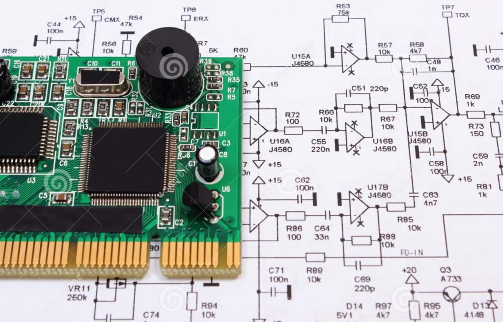
The manufacture of Printed circuit card after Printed circuit card reverse engineering service begin from the Epoxy Glass or similar substrate:
1st Image formation and transfer
The first step of Printed circuit card manufacture is establish the connection between the components. Manufacturer normally use the subtractive transfer to transfer the working film onto the metal conductor. This technology can lay a thin sheet of copper on it, and eliminate the residual copper. Additive pattern transfer is another method which has seldom be used after PCB wiring card reverse engineering.
Positive Photoresist is made by photosensible material, it can solve under the light, negative photoresist stands for those part which will solve without lighting. There are multiple ways to solve the photoresist on the Printed circuit card but the most commonly use method is heating it and rolling the surface where has been covered by the photoresist. It can use liquid way to spray on to it, however, the dry film can provide a higher resolution. Especially when cloning PCB card with extremely thin wires.
Light covering is just a template in the process of PCB reverse engineering and manufacturing, before the Printed circuit card go through the Ultra-violet exposure, those areas covered by the shield can prevent partial area won’t be exposed by the photoresist, presume this is the positive photoresist. These areas where have been covered by photoresist will be the layout.
After the development of photoresist film, other areas where requires to be etched away will be exposed. In the process of etching, Printed circuit card will be dip into the etching solution or spray the solution onto these Printed circuit cards. The most commonly used solution for etching will include Ferric Chloride, Alkaline Ammonia, Sulfuric Acid + Hydrogen Peroxide, Cupric Chloride, etc. remove the residual photoresist after etching process is done which has been called the STRIPPING process.
Tags: pcb assemble replicating,pcb board replicating,pcb card replicating,pcb replicating,pcba replicating,printed circuit board replicating,printed wiring board replicating,pwb replicating,pwba replicating