

Printed Circuit Board Reverse Engineering Process
Simply speaking, Printed Circuit Board reverse engineering process include from electronic component dismount, list and rationally display them, scanning the TOP & BOTTOM layer, if multilayer printed circuit board need to scrub the surface to get rid of the copper foil and show the existence of internal layer copper pattern, compile the circuit diagram and convert into Printed circuit board layout file, manufacture & assemble, functionality test according to customer requirement.
Printed Circuit Board Reverse Engineering Process
Hereby we can split the printed circuit board reverse engineering process into below parts:
First step: when you get a printed circuit board, you need to record all the electronic components designator, part number, parameter, especially for those diodes and triodes orientation and IC orientation. It is better to take some photos about the location of each component.
Second step: desolder all the electronic parts off printed circuit board and clean the residual tin trapped inside the PAD hole. Use alcohol to clean the printed circuit board surface and then install it under the scanning machine, higher pixel resolution is required when scanning the printed circuit board to have pictures with better quality.
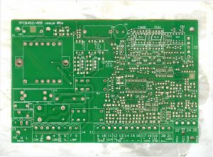
top side of PCB after desoldering all the components off the printed circuit board which going to be reverse engineered
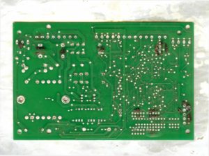
bottom side of PCB after desoldering all the components off the printed circuit board which going to be reverse engineered
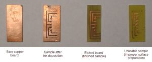
After that use sandpaper to scrub the TOP & BOTTOM layer slightly till the solder mask being completely removed from it and copper foil fully exposed, then we can scan the printed circuit board again under the scanning machine and start up PHOTOSHOP by colorful models.
top side of PCB after scrub off the solder mask from printed circuit board which going to be reverse engineered
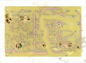
bottom side of PCB after scrub off the solder mask from printed circuit board which going to be reverse engineered.jpg
Third step: Adjust the canvas’s contrast ratio and light-dark ratio to ensure the part with and without copper foil has clear and strong contrast comparison. And then convert the picture into BLACK & WHITE model to inspect if all the wires are all clear and identified to guarantee the PCB layout drawing, gerber file and schematic diagram quality of printed circuit board reverse engineering process. After the inspection we can store the pictures in the format of BMP and if there is any problem being spotted we can use PHOTOSHOP to do the modification and rectification.
The forth step: convert the two BMP format files into PROTEL format files and input into the PROTEL software as two layers, if the PADs and VIAs which go through the two layers can be aligned properly means the steps mentioned above are all executed well. PCB reverse engineering is a very dedicated work which need much patience and carefulness, any minor error will affect the quality of work.
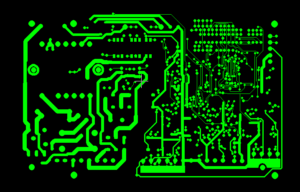
gerber file bottom layer of printed circuit board after reverse engineering
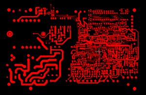
gerber file top layer of printed circuit board after reverse engineering
The fifth step: convert the BOM layer to TOP PCB and be sure the file should converted to SILK layer and then you can draw the circuitry wire on the TOP layer. After that we need to use laser printer to print TOP LAYER & BOTTOM LAYER onto the transparent film according to 1:1 ratio.
Tags: pcb assemble duplicate,pcb board duplicate,pcb card duplicate,pcb duplicate,pcba duplicate,printed circuit board duplicate,printed wiring board duplicate,pwb duplicate,pwba duplicate