

Printed Circuit Board Design
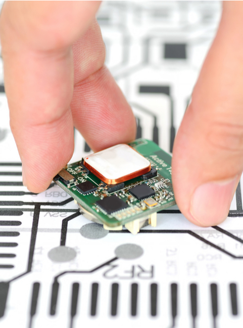
In hardware design, Printed Circuit Board Design is a very important and indispensable step. For some simple products, PCB design may simply connect all devices and networks correspondingly. For high-speed printed circuit board reverse engineering and radio frequency circuits of clone pcb circuit card, the design of PCB directly affects whether the functions of the product are normal and whether the product can meet the requirements of entering the market.
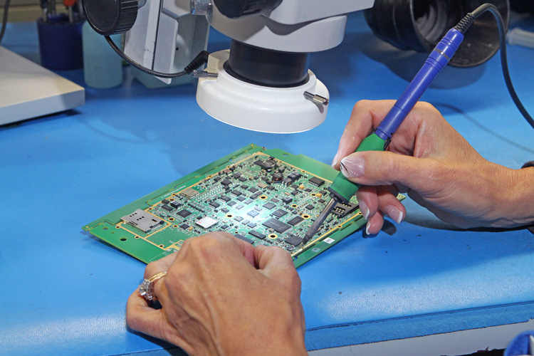
Below, the PCB design process, copying PCB layout diagram, PCB wiring, and PCB design checklist will be introduced. The quality of the PCB directly determines whether an electronic product is good or bad, so a good PCB design process is crucial and important.
Many engineers think that PCB design is simply to arrange all the components and then connect all related device pins together. This is a narrow point of view. A good PCB design procedures starts from the design of the principle scheme, such as how to choose the right scheme, choose the right electronic components, etc.