

PCB Reverse Engineering Tools
PCB reverse engineering is a detailed and technical process that involves extracting design data from an existing physical printed circuit board to recover, restore, or recreate its original schematic diagram, layout drawing, and Gerber files. Whether the goal is to remanufacture a legacy product, duplicate a discontinued board, or redesign a current circuit for improvement, using the right tools is critical for accurate and efficient work.
Below is an overview of essential tools used in PCB reverse engineering, along with the tasks they support throughout the reverse engineering workflow.
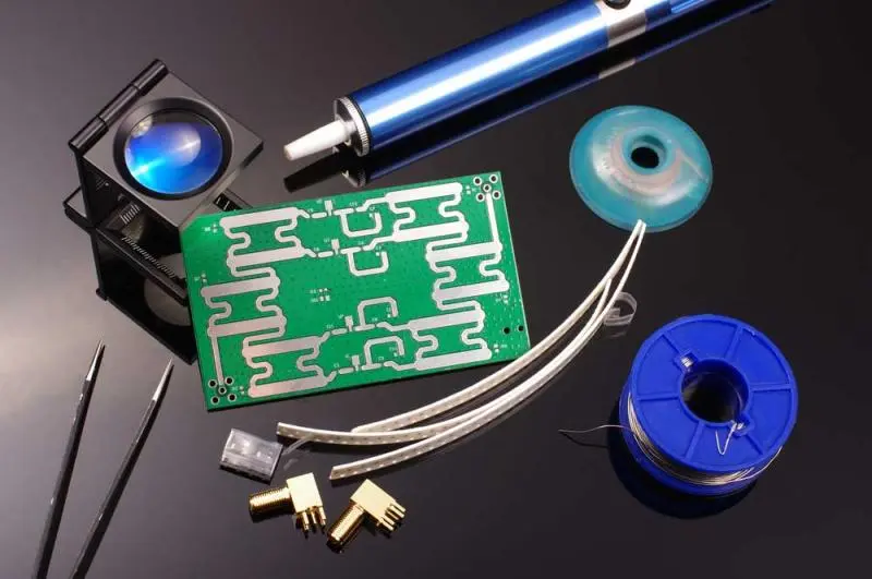
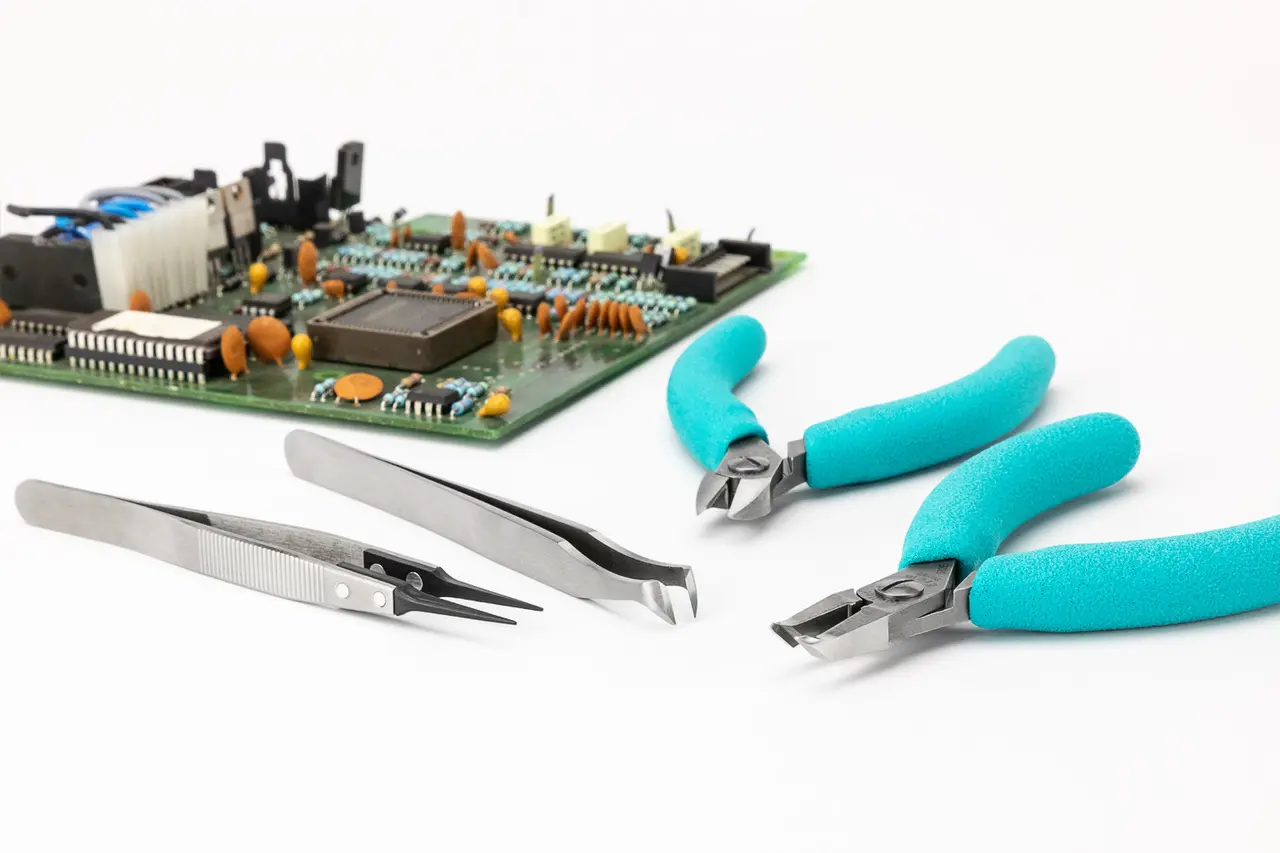
1. High-Resolution Scanners and Microscopes
High-resolution scanners and optical microscopes are used to scan and inspect both sides of a PCB to identify track patterns, component placements, and label markings. These tools help replicate the board’s layout and create reference images for manual tracing or digital reconstruction.
2. X-ray Inspection Systems
For multilayer PCBs, especially those with BGAs or buried vias, X-ray imaging is essential. It allows engineers to recover internal connections that are not visible on the surface. This step is crucial for reproducing complex netlists and reconstructing hidden signal paths.
3. EDA Software Tools (Electronic Design Automation)
Tools such as Altium Designer, KiCad, Eagle, and OrCAD are used to draw schematic diagrams, build layout drawings, and export Gerber files and BOM lists. These applications allow for precise cloning or redevelopment of the PCB by digitally recreating the original board structure.
Key capabilities include:
- Schematic Capture – To recreate and visualize the electrical relationships between components.
- PCB Layout Editor – To design or duplicate the physical layout of the board.
- Netlist Generation – To verify and compare connections extracted from the original board.
- Gerber File Export – For manufacturing-ready data output.
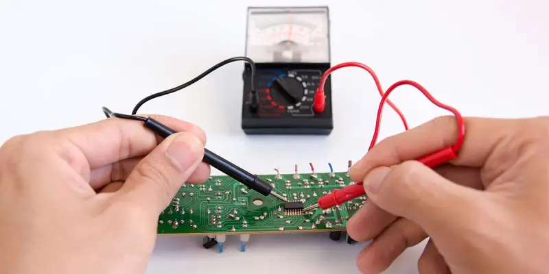
4. Multimeter and Oscilloscope
To test and verify signal paths and component behavior, tools like multimeters and oscilloscopes are used during the reverse engineering process. They help engineers refurbish or validate the board’s electrical performance after reproduction.
5. BOM Extraction and Analysis Tools
Specialized software and component identification tools help recover and rebuild the BOM list, identifying resistor and capacitor values, IC types, and footprints, which is vital for sourcing and remanufacturing the board.
Conclusion
From manual inspection to digital design software, the tools used in PCB reverse engineering are essential to successfully replicate, restore, or redesign electronic circuit boards. With the right setup, engineers can efficiently reproduce or clone legacy PCBs, ensuring functionality, compliance, and manufacturability.
PCB Reverse Engineering Tools will require a set of tools to complete the job, so it is important that adequate hardware be available as early as possible to develop the necessary data through reverse engineering process. The number of parts required varies greatly with the complexity of the part and the testing requirements.
The quantity of tools required for pcb reverse engineering should be determined depending upon complexity and risk assessment. Such as high frequency product, and its PCB will always has high frequency inductor which will need professional device to detect the value and specification and the manufacture prototype.
Consideration should be given to the possible destruction of an item during disassembly and material analysis. Whenever possible, only new items from inventory should be used as it is difficult to establish performance criteria or tolerances on used parts. The use of new items from inventory precludes the pcb reverse engineering process from resulting in an unsuitable part, due to existing defects. It may be necessary at times, to obtain the tools from other sources such as field units or commercially available items direct from the vendor.
As an dedicated service provider for PCB Reverse Engineering, Circuit Engineering Co.,Ltd has a bunch of professional tools and hardwares which will help our customer obtain high level of satisfactory over their project.
Tags: pcb reverse engineering hardware,pcb reverse engineering technical