

PCB Clone Accuracy
When it comes to PCB clone accuracy, achieving high precision is critical to the success of any reverse engineering or reproduction project. Whether the goal is to recover, restore, recreate, or remanufacture an existing electronic design, maintaining the fidelity of the Gerber files, schematic diagrams, layout drawings, BOM lists, and netlists is essential to ensure that the cloned PCB performs exactly like the original.
The Importance of PCB Clone Accuracy
PCB clone accuracy is not simply about copying the physical appearance of a circuit board. It’s about deeply understanding the electrical functionality, material characteristics, signal integrity, and mechanical structure of the original design. Even a slight deviation in the layout drawing or errors in the BOM list can lead to major failures in product performance, safety, or reliability.
In industries such as aerospace, medical devices, UAVs, and automotive electronics, where precision is vital, PCB clone accuracy must meet or exceed the original standards. A cloned PCB must replicate not just the visible circuitry but also hidden features like internal layers, impedance control structures, and thermal management strategies.
Key Steps to Ensure High PCB Clone Accuracy
Comprehensive Reverse Engineering Process
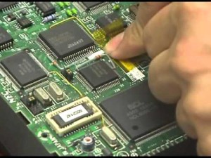
The cloning process starts with professional reverse engineering. Engineers carefully inspect the physical PCB, copy the design, and recover important data such as board dimensions, layer count, and component placement. Tools like X-ray inspection, 3D scanning, and microscopic imaging are often used to expose hidden structures.
Accurate Gerber File and Netlist Creation
Generating precise Gerber files is essential. These files define the copper layers, solder mask, silk screen, and drill data. Along with this, an accurate netlist must be restored or recreated to ensure that all electrical connections match the original circuit perfectly.Schematic Diagram Reconstruction
A schematic diagram is redeveloped to represent the logic and functionality of the original design. This schematic acts as the blueprint for the entire system and must correctly reflect component relationships and signal flow.BOM List Refinement
An accurate BOM list (Bill of Materials) is critical to the cloning process. Every component—resistors, capacitors, ICs, connectors—must be correctly identified, duplicated, and, if necessary, refurbished or substituted with equivalent parts without affecting functionality.Prototype Reproduction and Testing
After the design files are completed, a prototype PCB is reproduced and subjected to rigorous testing. Electrical, mechanical, and environmental tests ensure that the cloned PCB matches the original in all aspects.
Common Challenges in Achieving PCB Clone Accuracy

Complex multilayer designs with blind and buried vias increase the difficulty of accurate data extraction.
Proprietary components or encrypted ICs may require deeper analysis or custom replacements during redevelopment or redesign.
Aging PCBs with worn traces or damaged parts can make the recovery of accurate schematics and layouts more challenging.
As we all know, PCB Clone Accuracy depends on the preciseness of image scanning, so high DPI makes lots of sense in the scanning image, but DPI can’t set too high to undertake by computer because the higher the DPI value, the larger image it will have after scanning, so the DPI value had better being set according to the density of pcb;
2nd is the tolerance of scanner, it is almost impossible to find a scanner exempt of any tolerance, and most of scanners will have tolerance in one orientation, sometimes will have two orientations, but all of these tolerances can’t be found by human eye even load and check by PHOTOSHOP, so generally speaking if the pcb line width or space is within MIL could be very difficult to find these tolerances;
The last thing comes to the processing of scanning pictures, operators without sufficient care will usually cut out more or less several millimeters and it could be a real problem for subsequent pcb clone especially double side pcb or multilayer pcb;
Summary all the points above we can conclude the selection of pcb clone software must take these points into consideration like whether or not cutting pictures is required, whether or not the adjusting functions for scanning tolerances is possessed, as well as the layer alignment functions.
Tags: pcb assemble clone,pcb assembly clone,pcba clone