

PCB Circuit Board Layout Drawing Reverse Engineering
Faced with the increasingly high integration of hardware platforms and increasingly complex systems of electronic products, PCB Circuit Board Layout Drawing reverse engineering should be modularized, and modularity should be used both in the design rebuilding of hardware schematics diagram and printed circuit board layout file, structural design method.
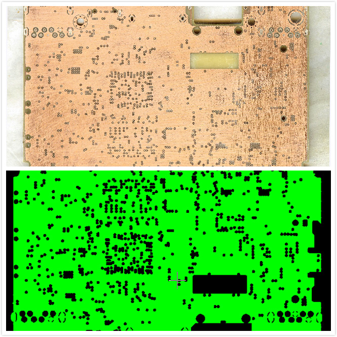
As a hardware engineer, under the premise of understanding the overall architecture of the system, you should first consciously integrate modular design ideas in the process of reverse engineering circuit board schematic and PCB layout design, and plan the basic ideas for PCB layout based on the actual situation of the PCB.
The placement of fixed components is similar to the placement of fixed holes, but also pay attention to a precise location. This is mainly placed according to the design structure. Center and overlap the silk screen of the component and the structure, as shown in below Figure.
After the fixed components on the board are placed, the signal flow of the entire board can be sorted out according to the principle of flying line proximity and signal priority.